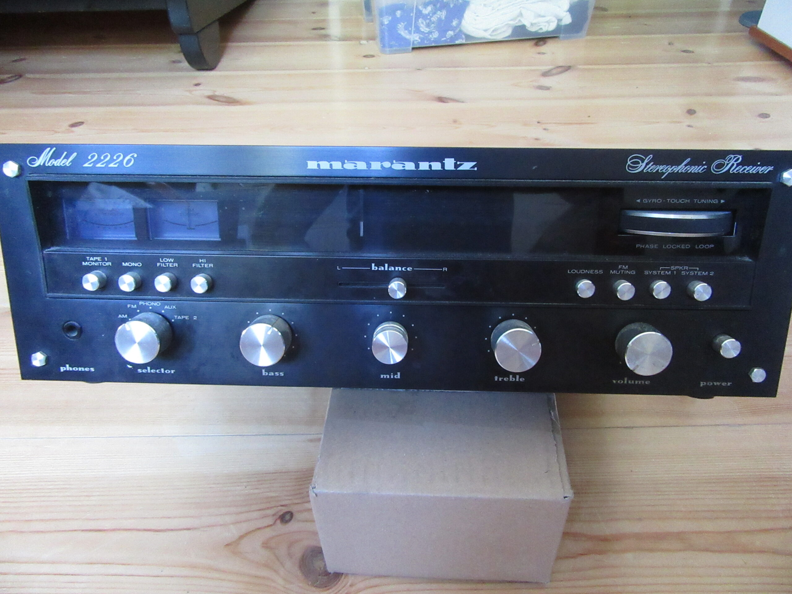
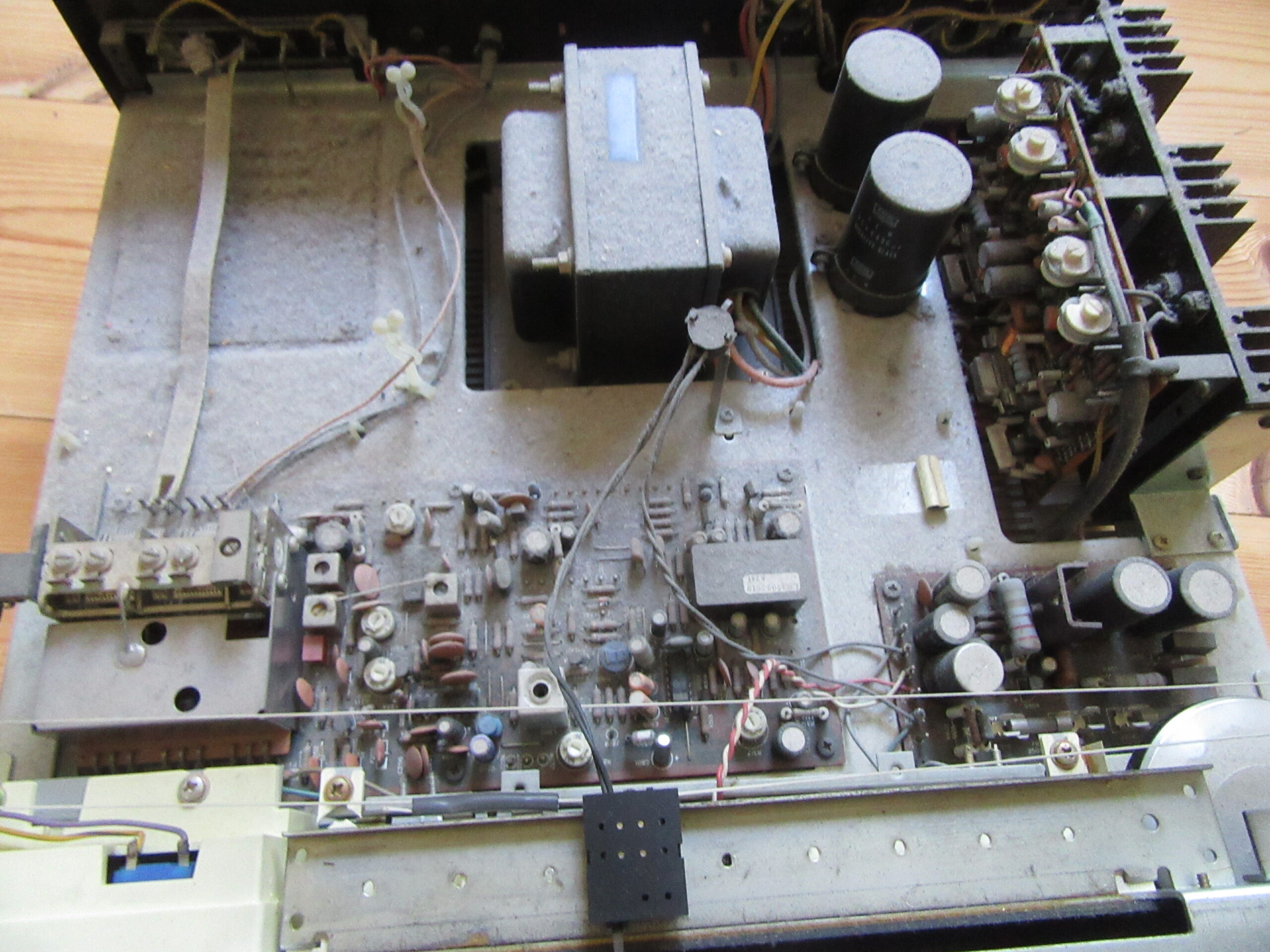
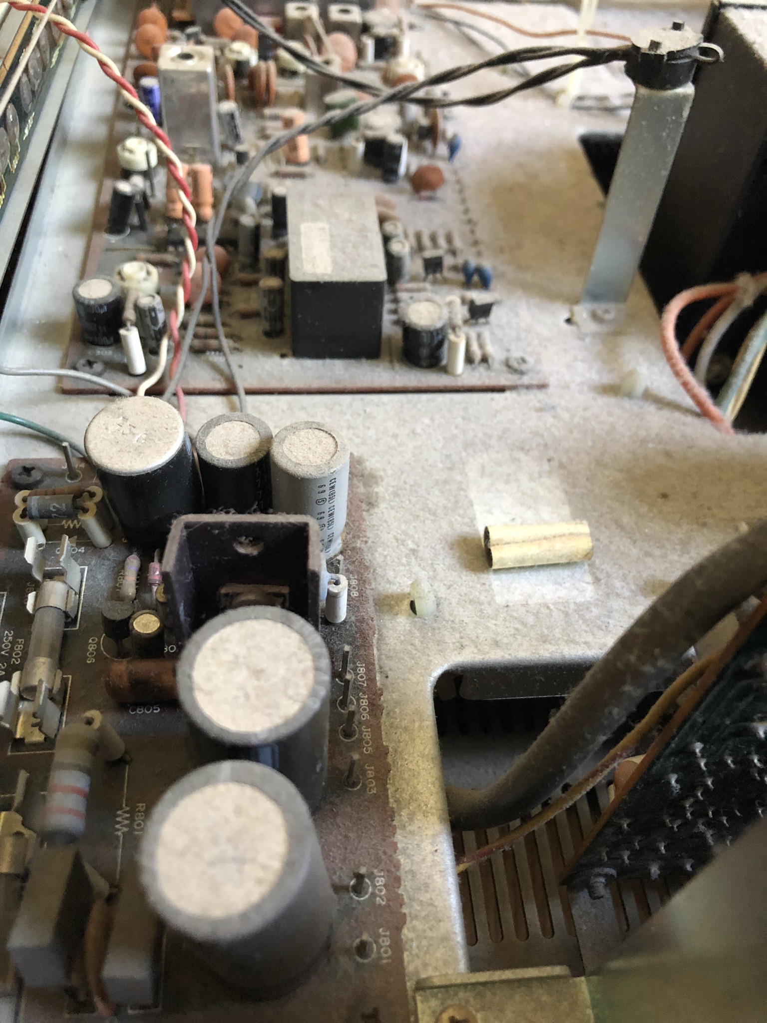
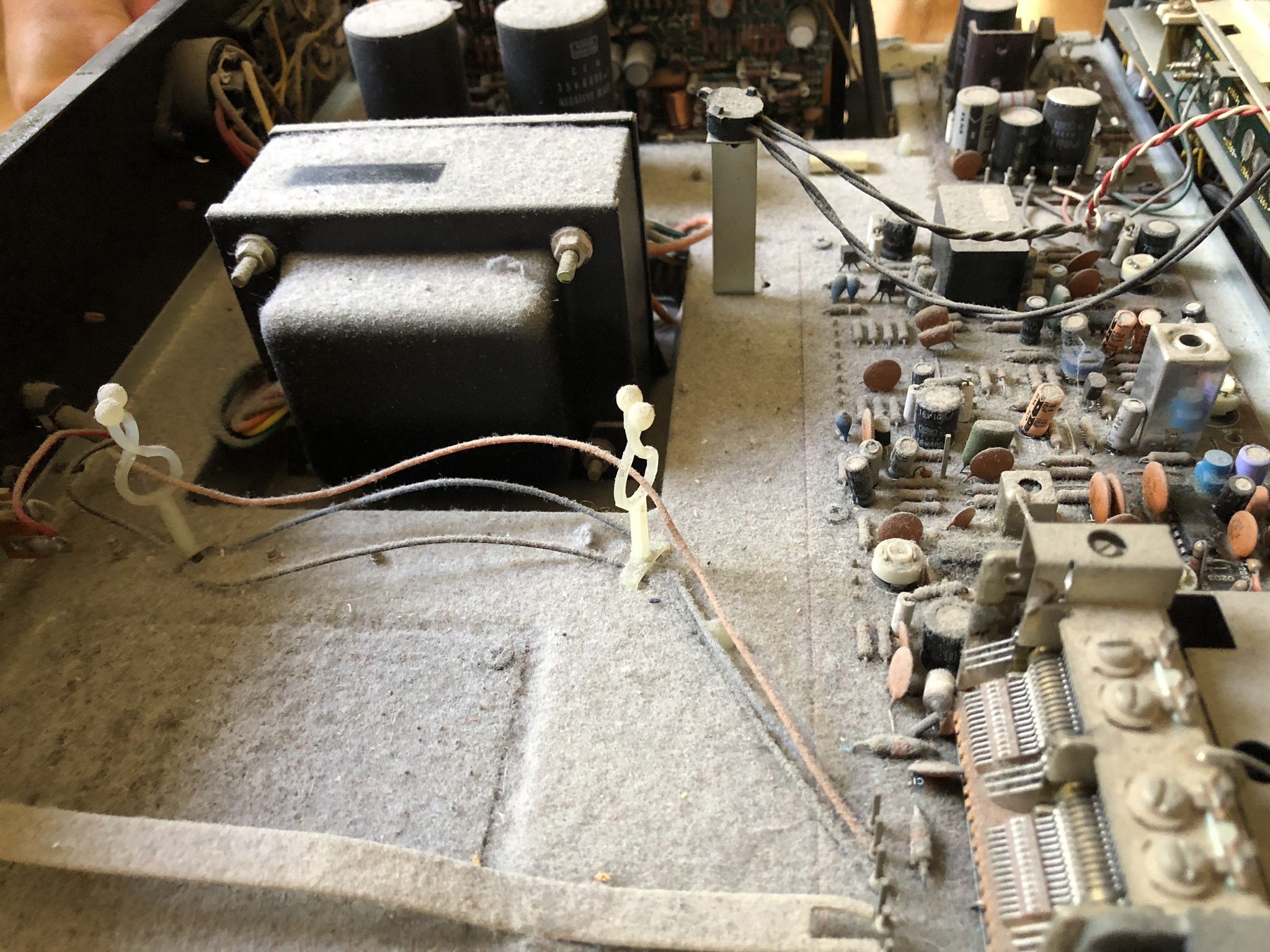
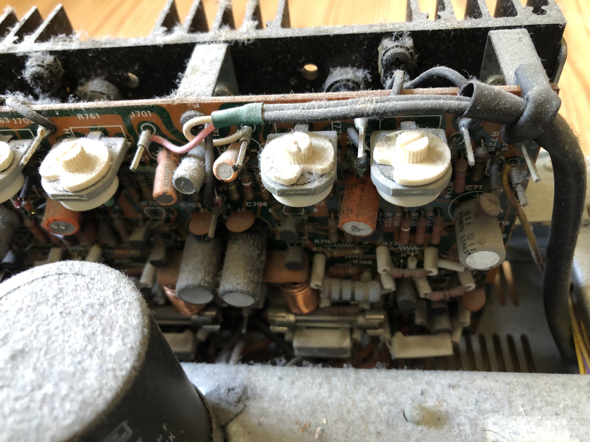
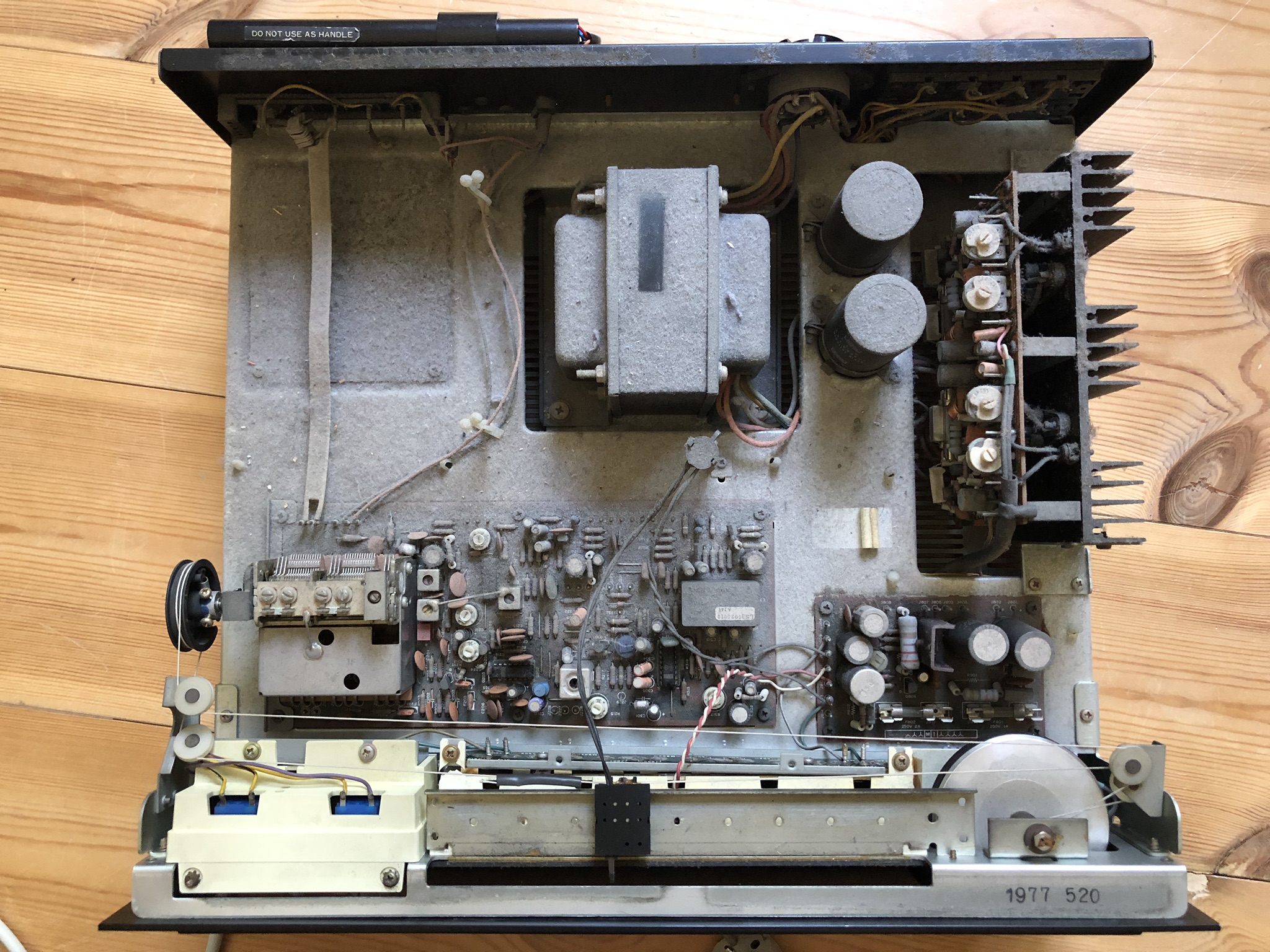
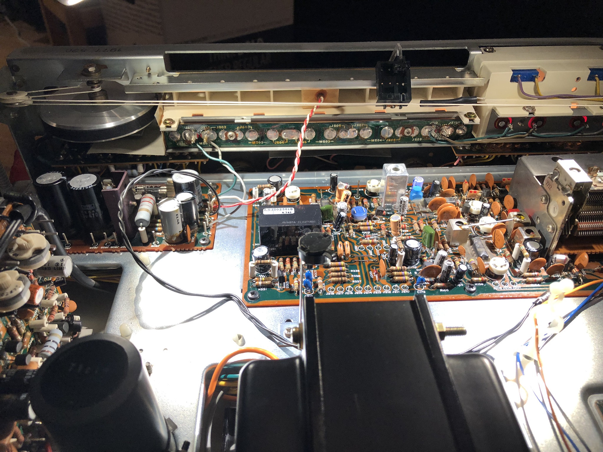
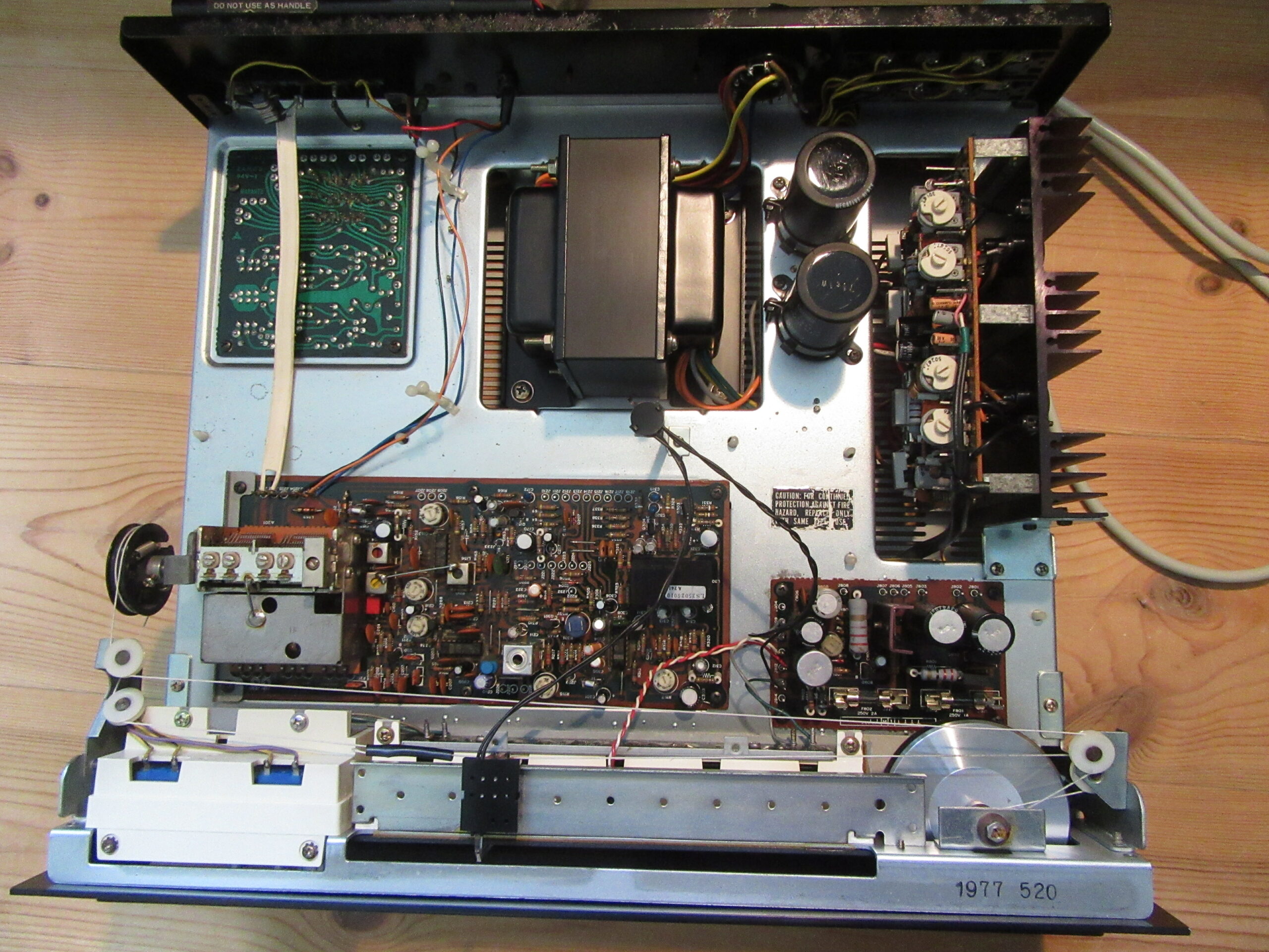
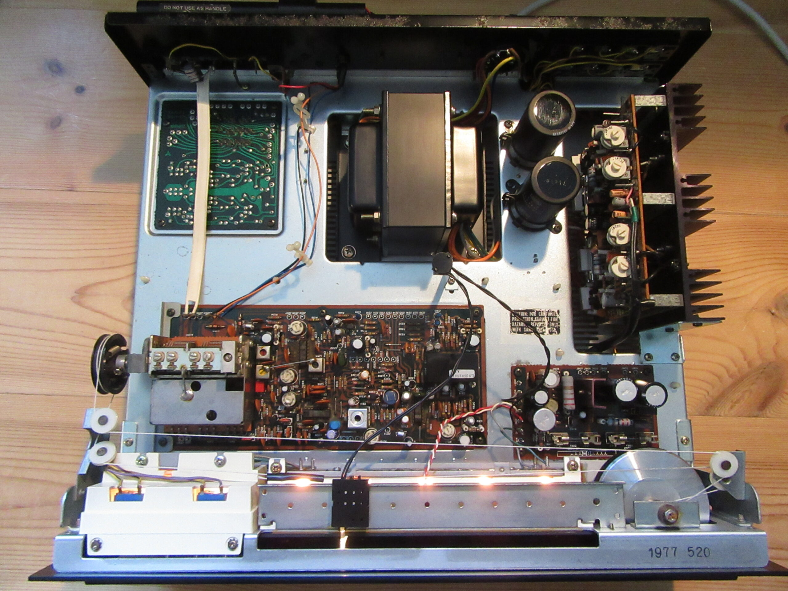
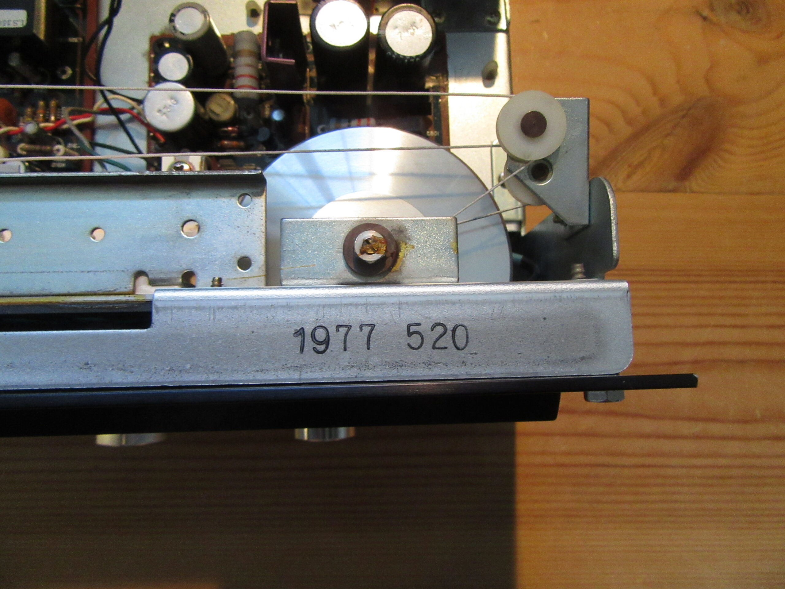
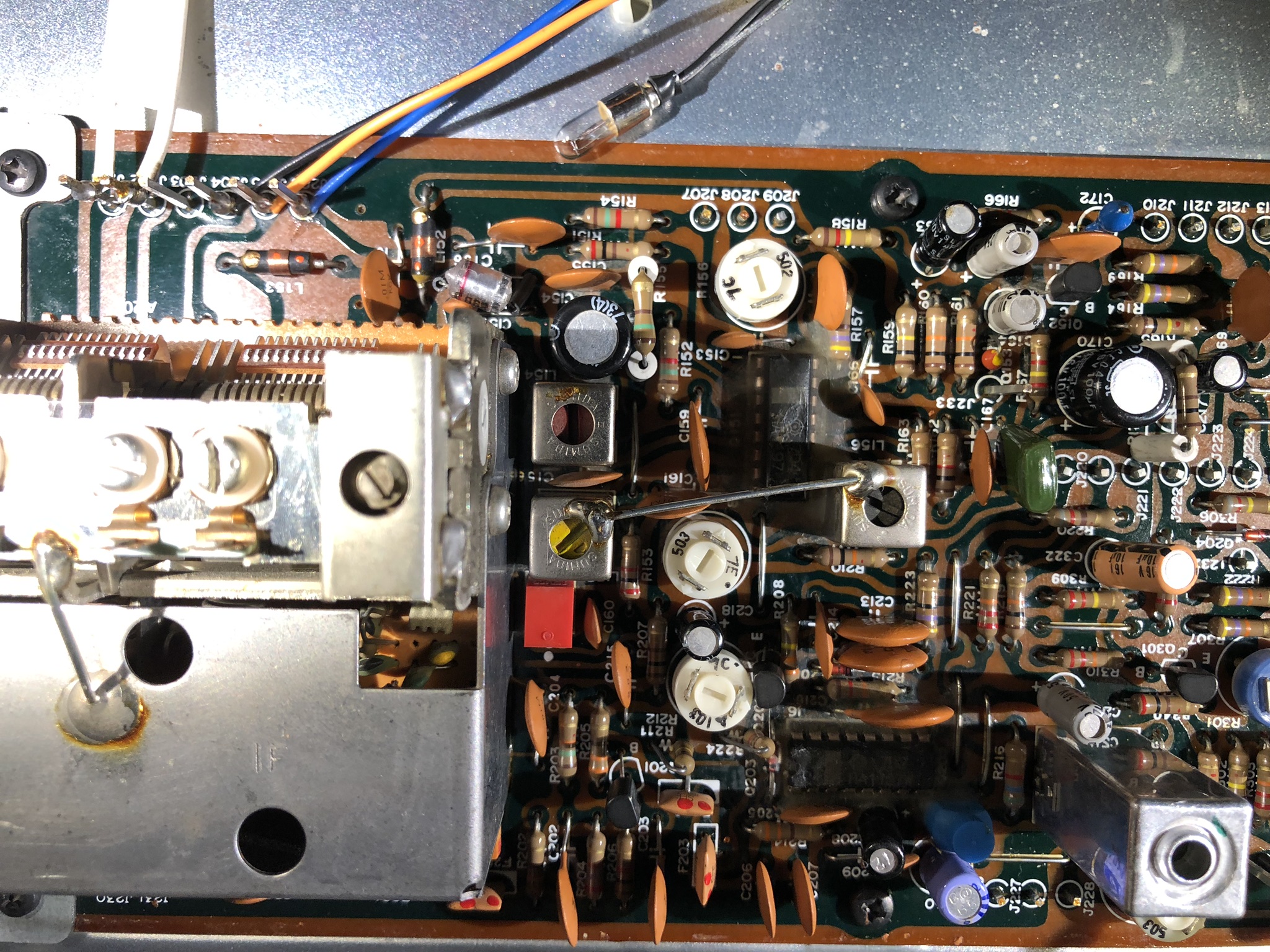
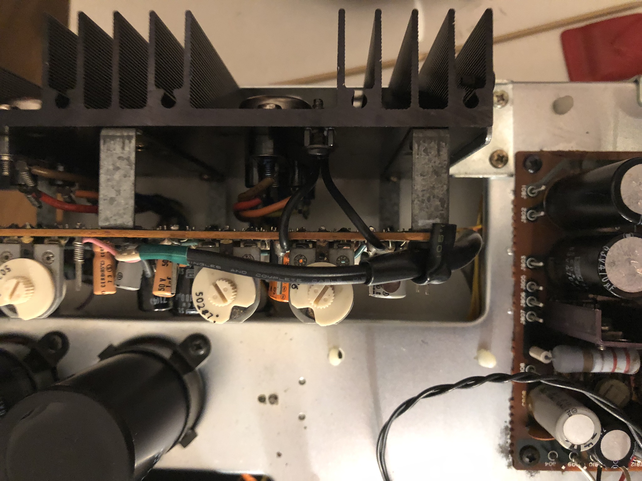
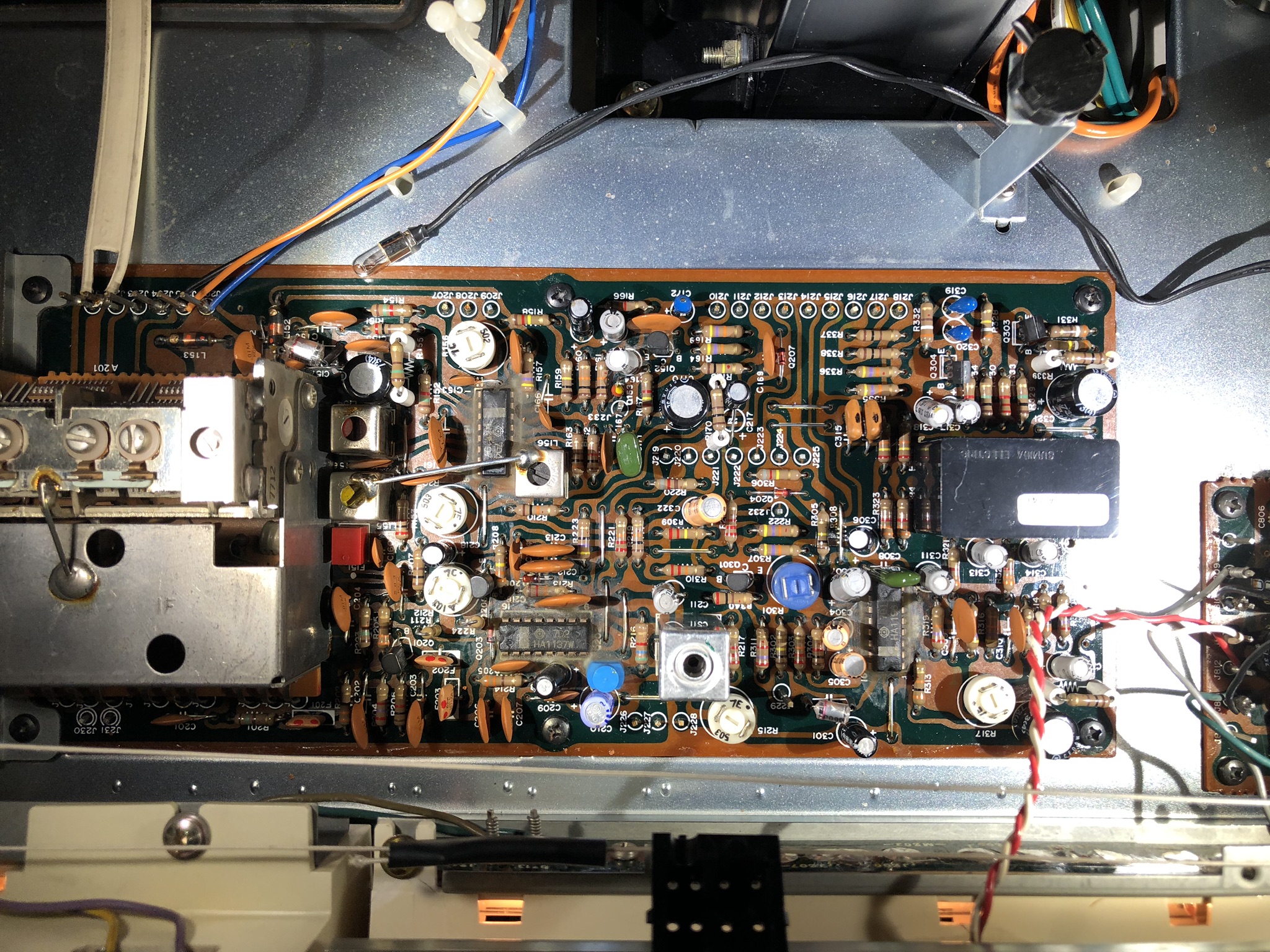
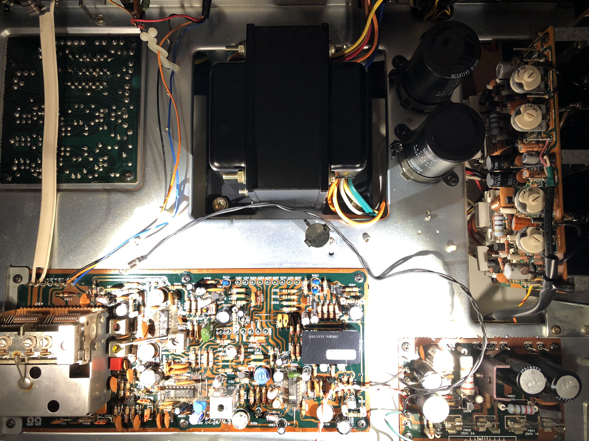
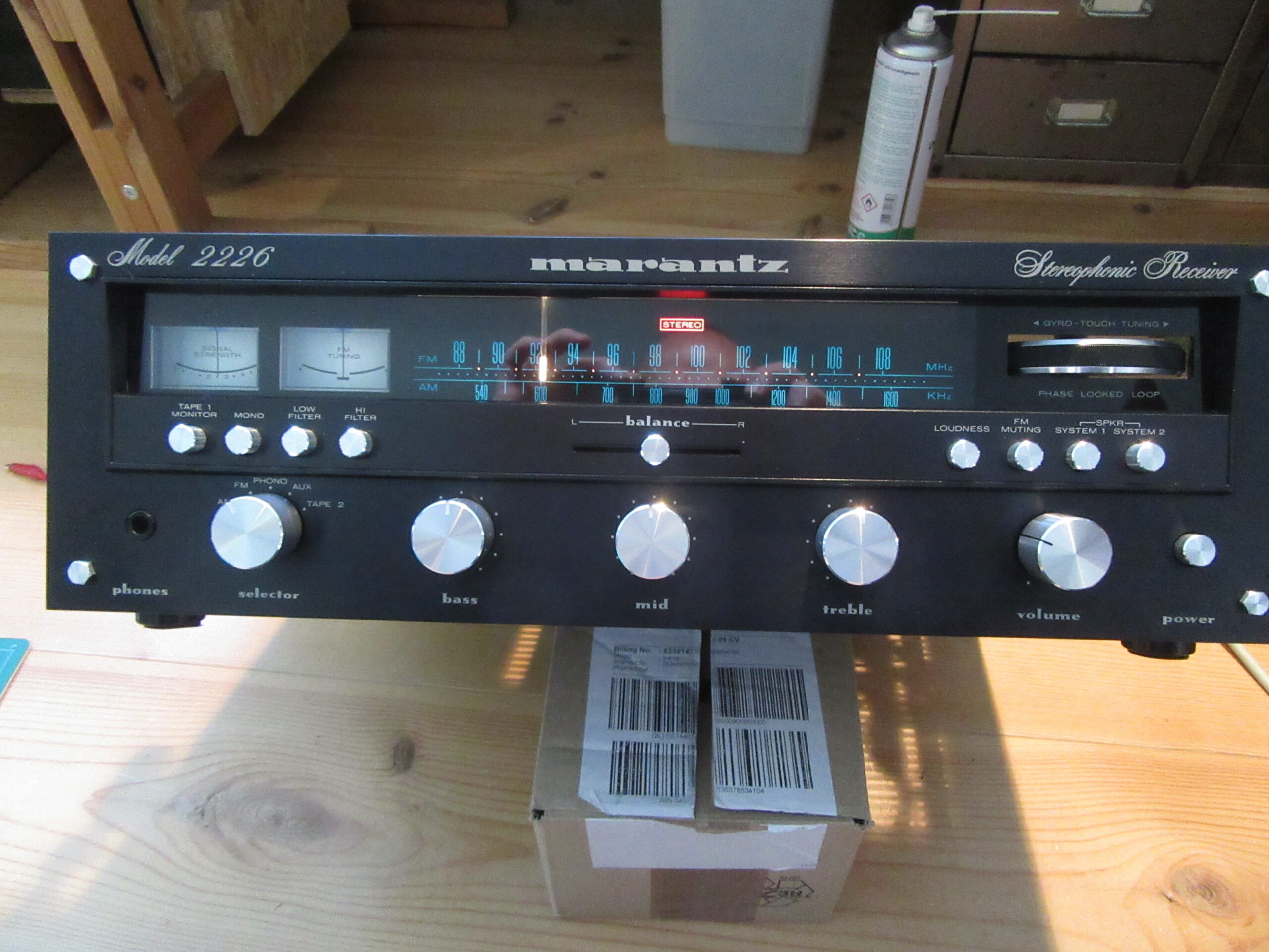
The unit was in excellent condition after 42 years of operation, so the restoration consisted mainly of a meticulous cleaning. Nevertheless, a few small things had to be fixed
one of the big knobs was no longer original
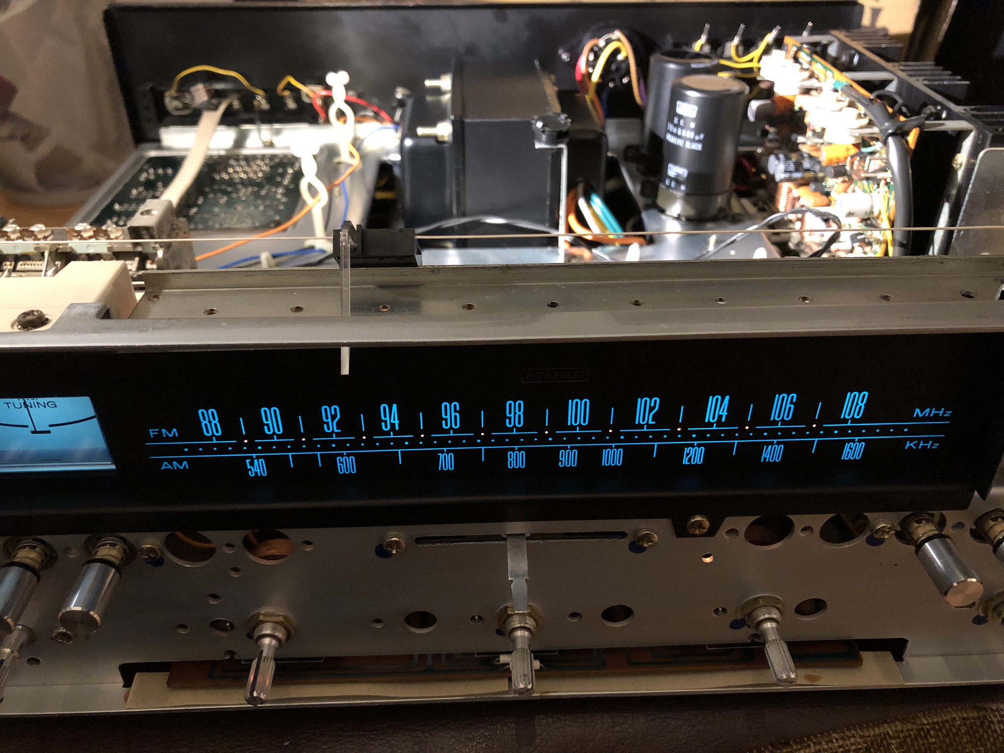
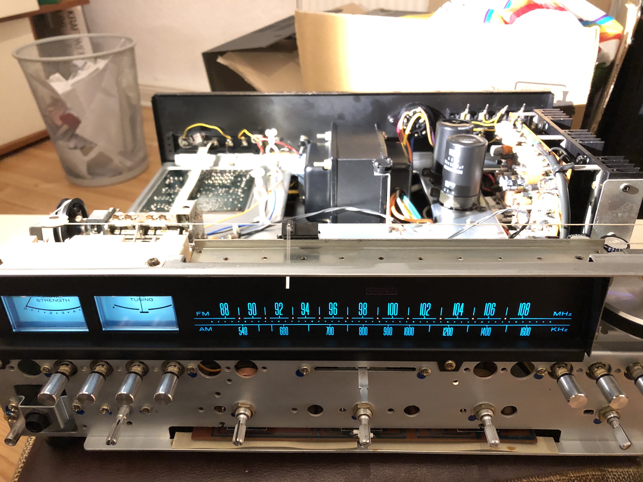
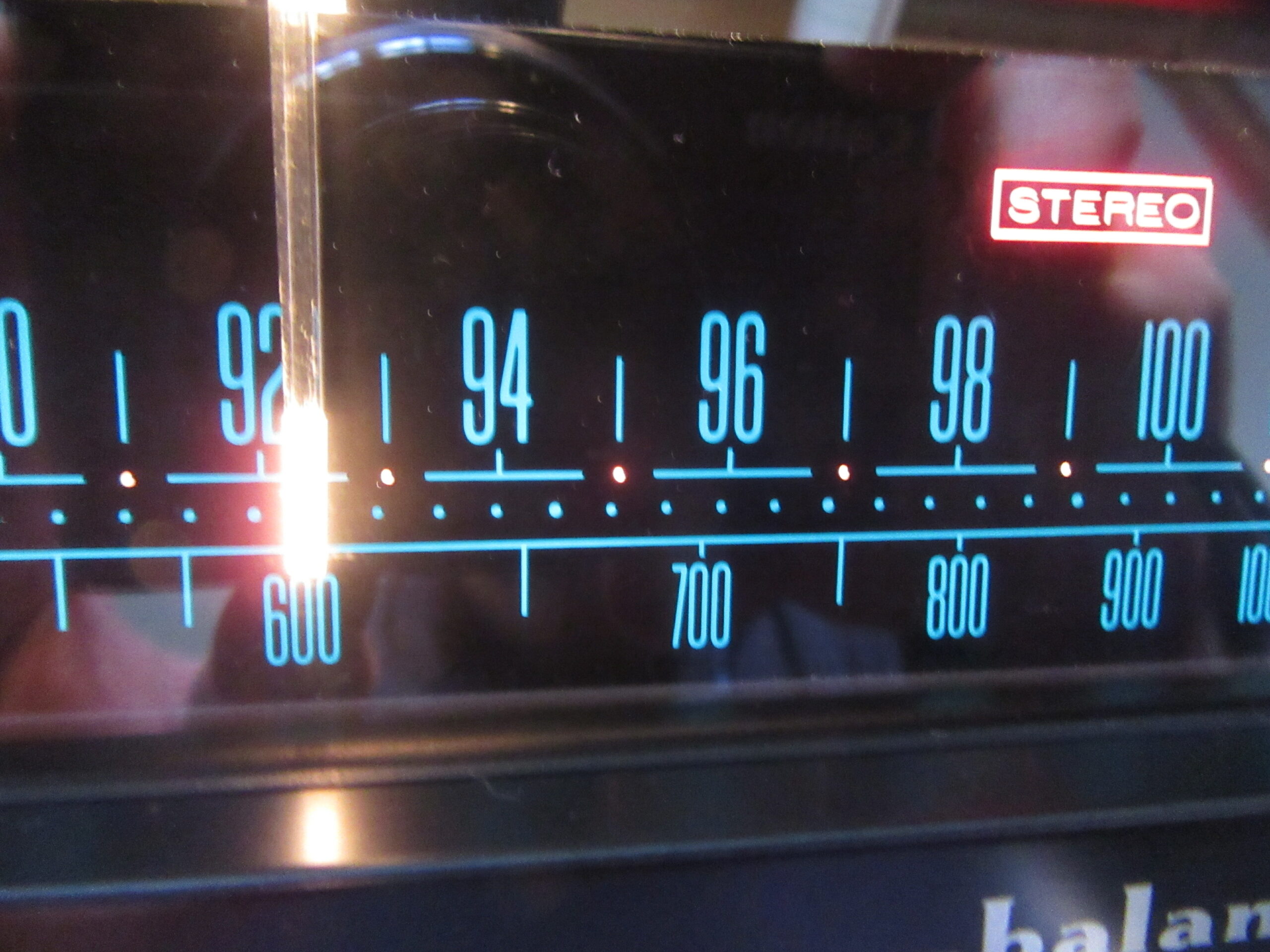
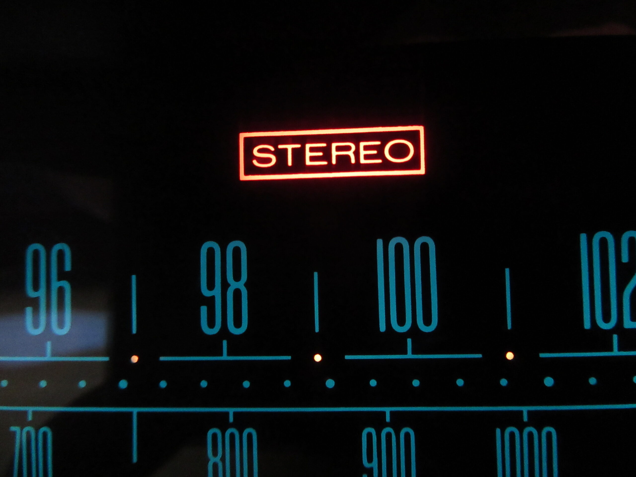
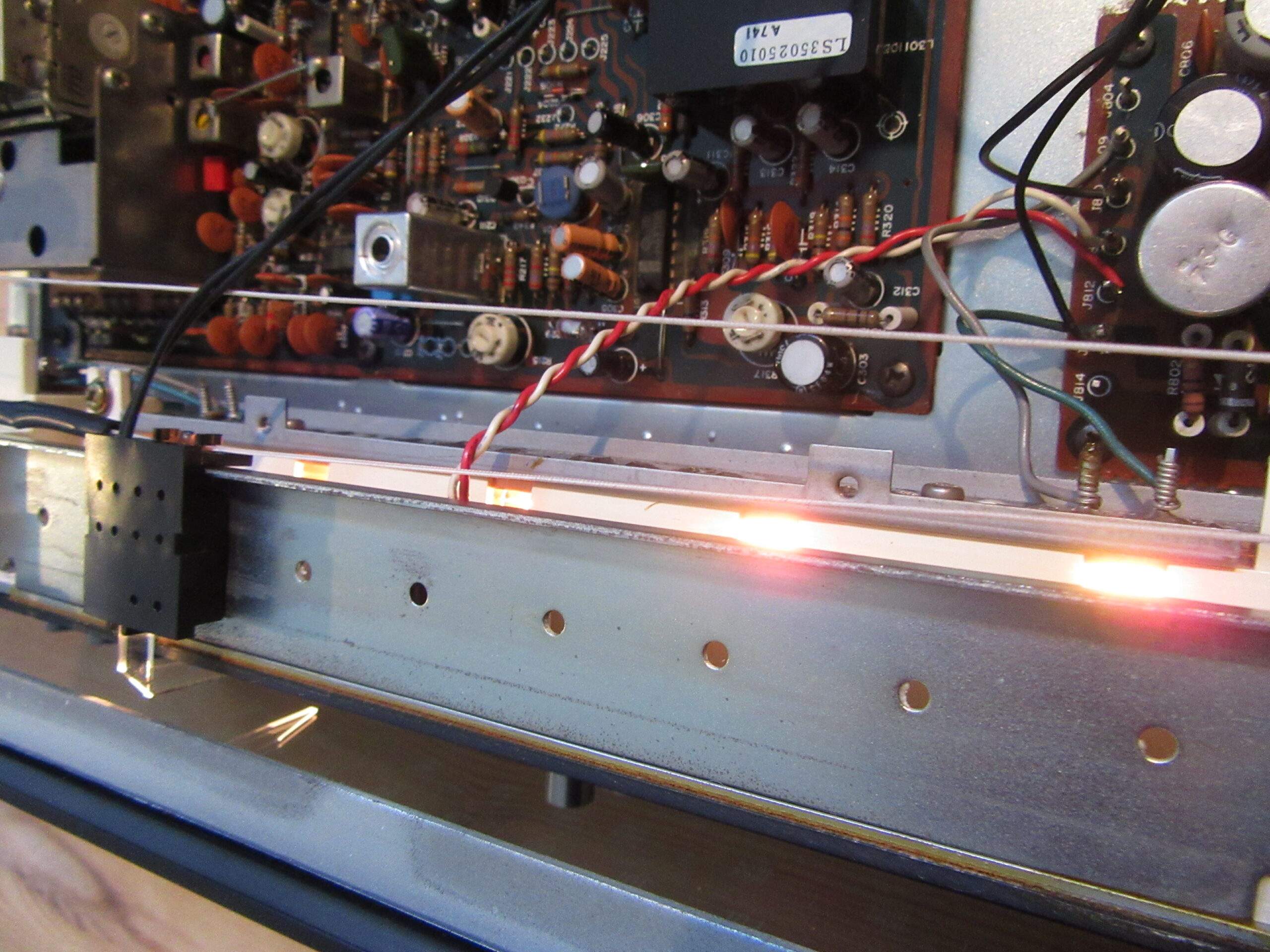
the dial illumination was defective
squeaking noises during tuning
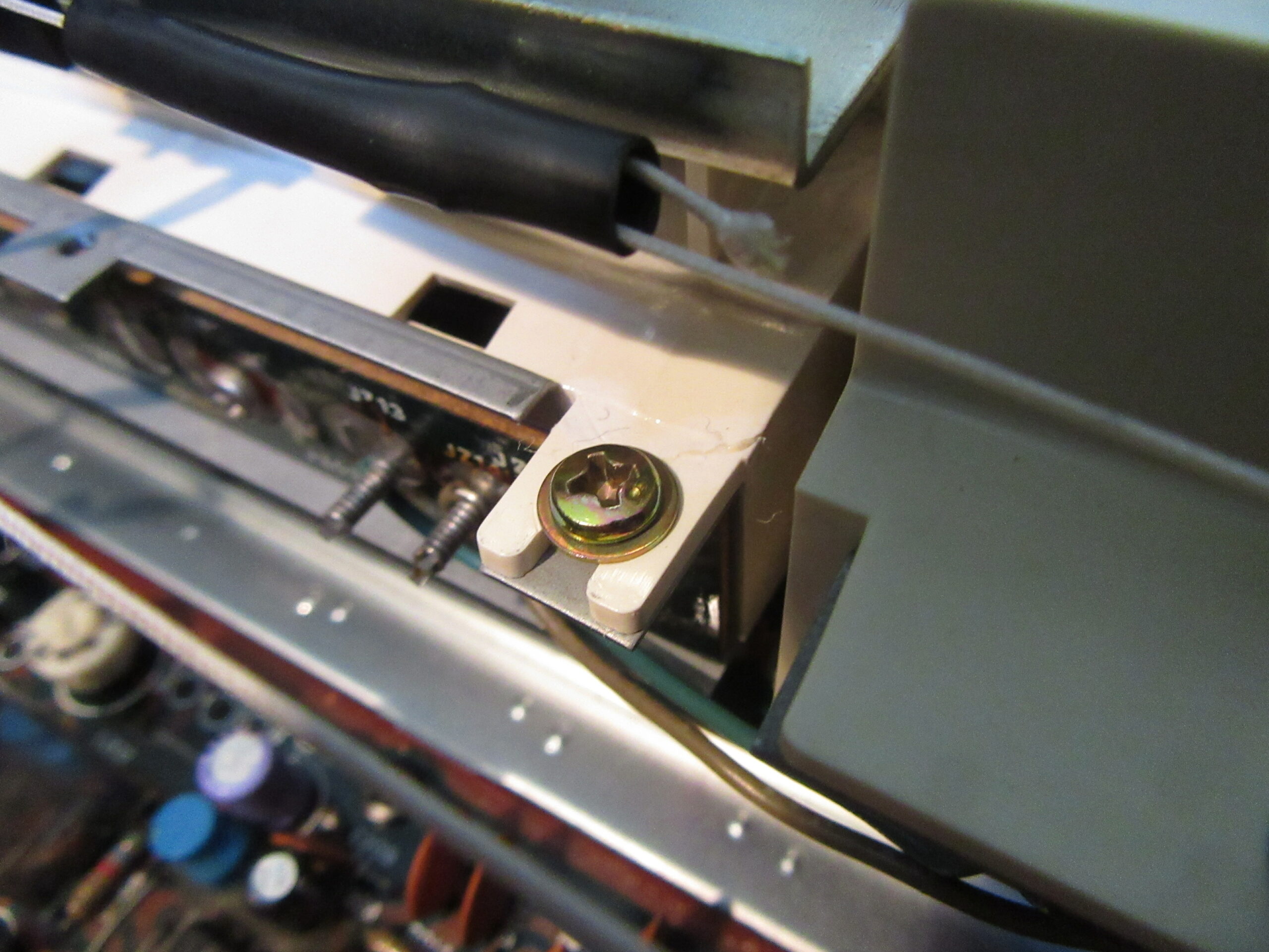
broken off plastic corner at the scale holder
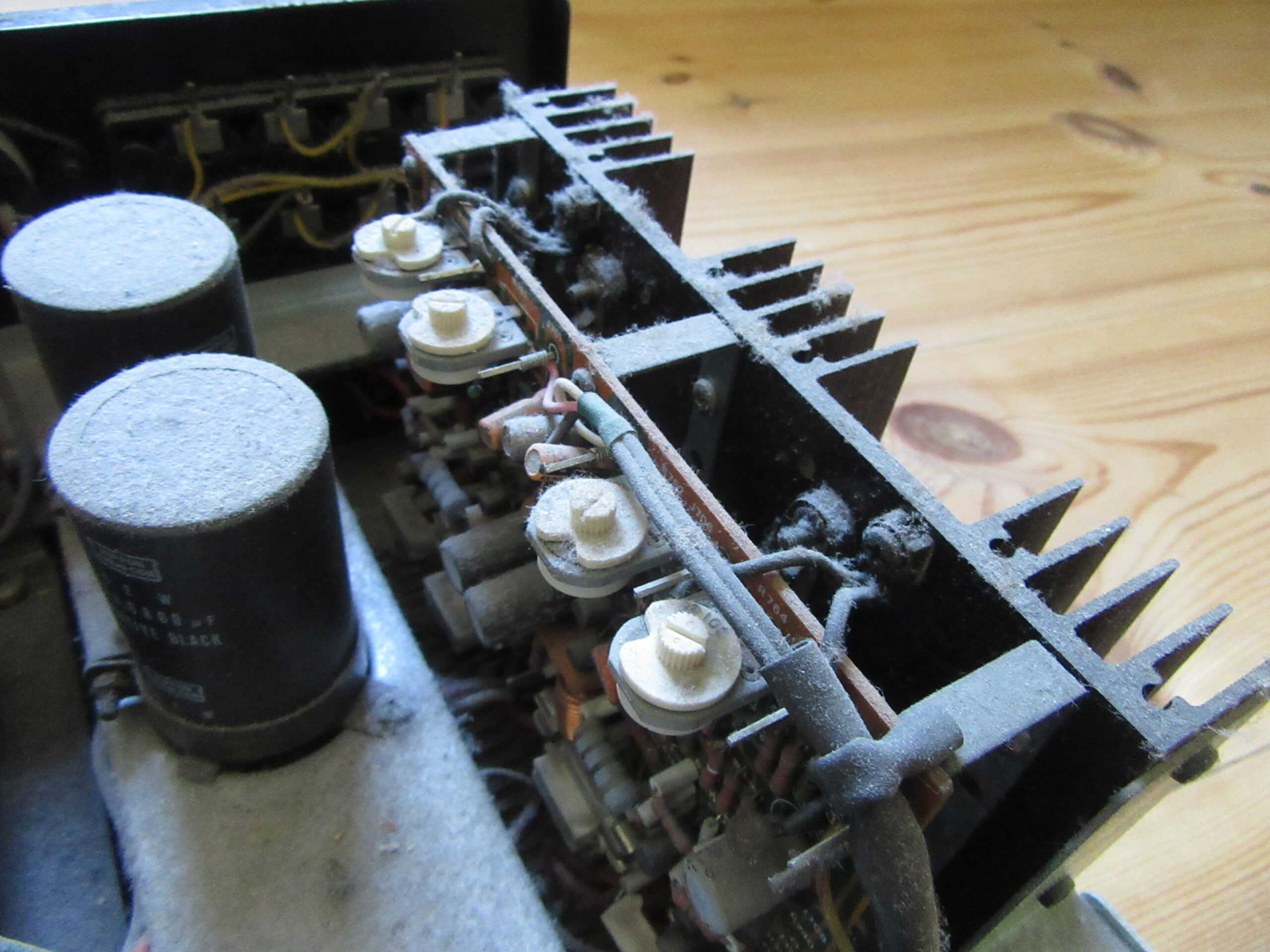
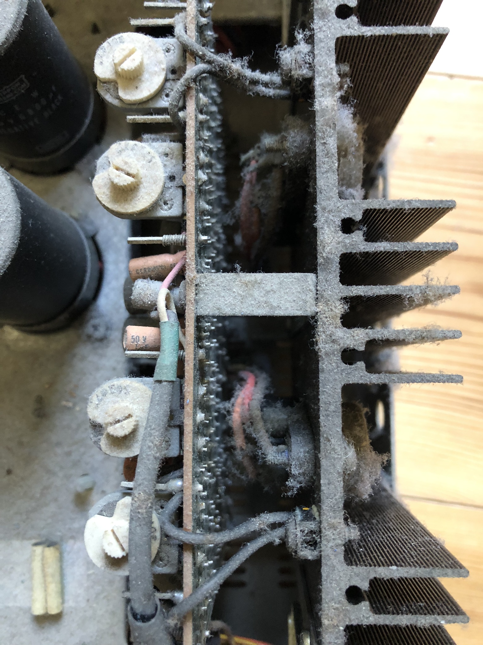
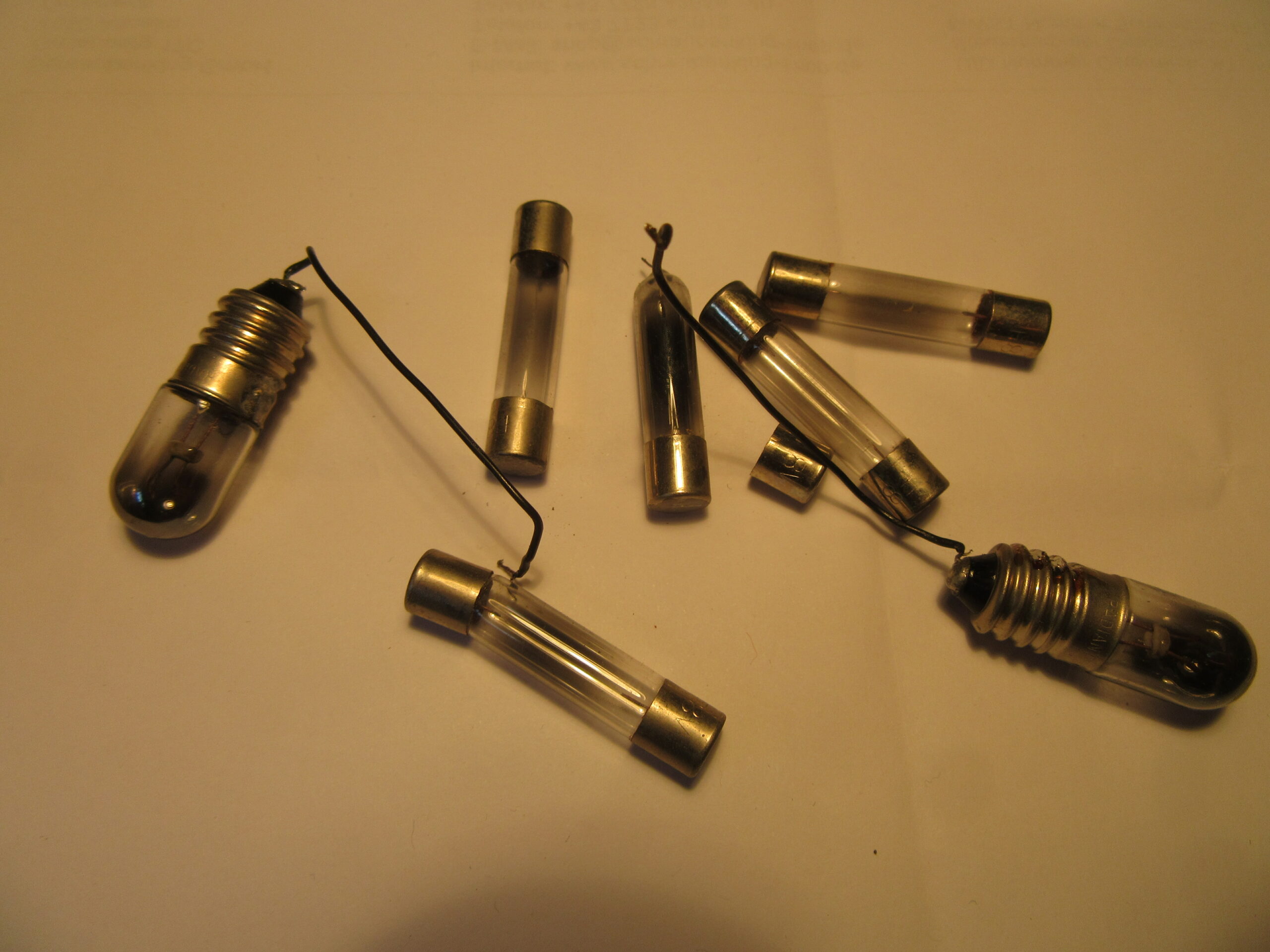
I found a new original knob on the internet for an outrageous 10 Euro or so. For the scale illumination I replaced the 6x30mm 8V pilot bulbs with 12V versions. This makes the illumination darker, but it lasts forever and the plastic parts are no longer stressed by heat. I also reversed the unconventional conversion to E10 bulbs. I got rid of the squeaking noises by using Ballistol on the idler pulleys. And the broken off plastic corner I glued back on with rather toxic Dichlormethane. The potentiometers had only a slight scratching, so nothing has been done here yet. That will be repaired in 30 years.
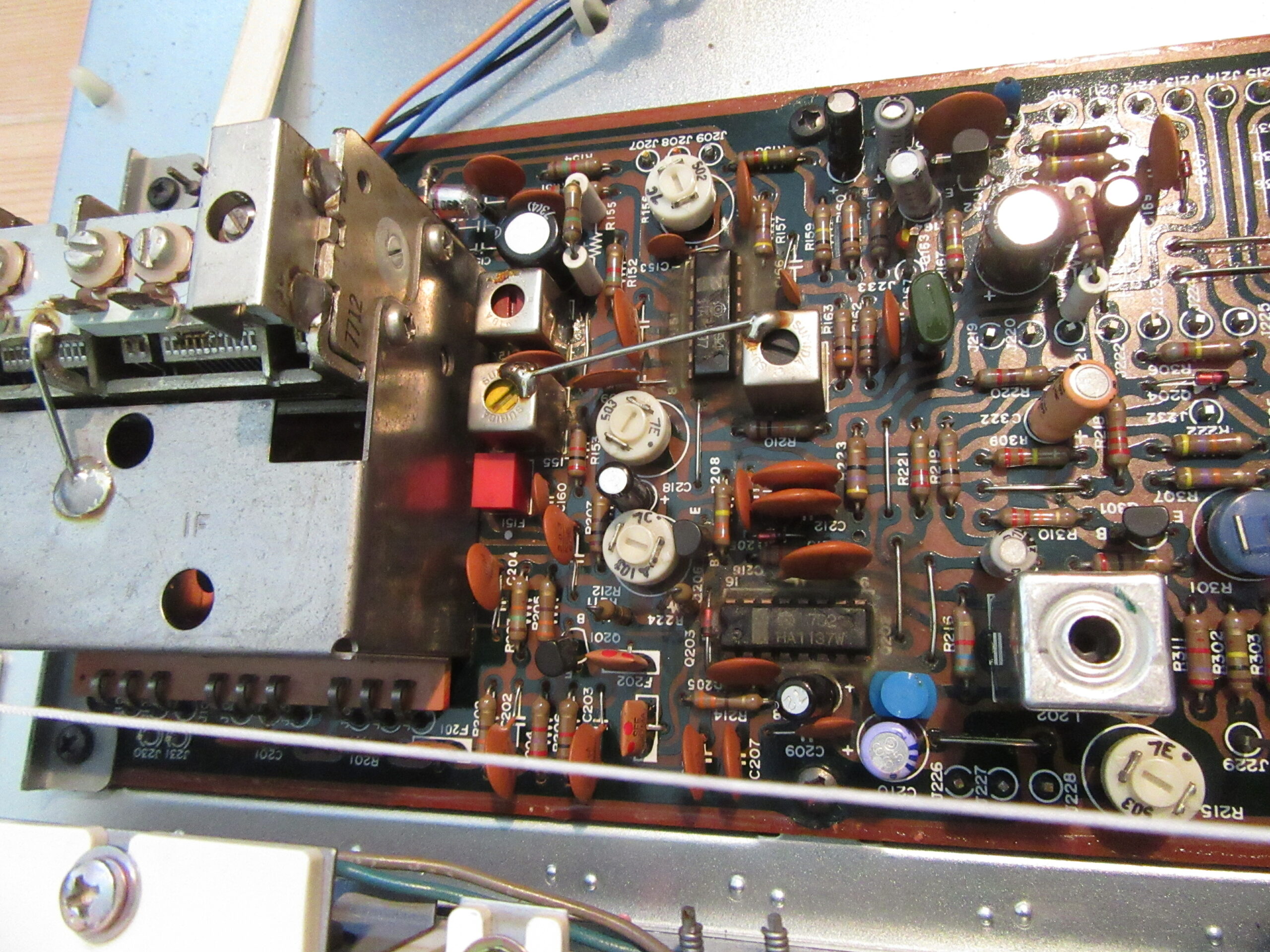
During cleaning I moved a 78XX voltage regulator with heat sink too much. This caused a hairline crack to form next to the solder joint and of course the receiver stopped running. But the fault was quickly found and fixed.
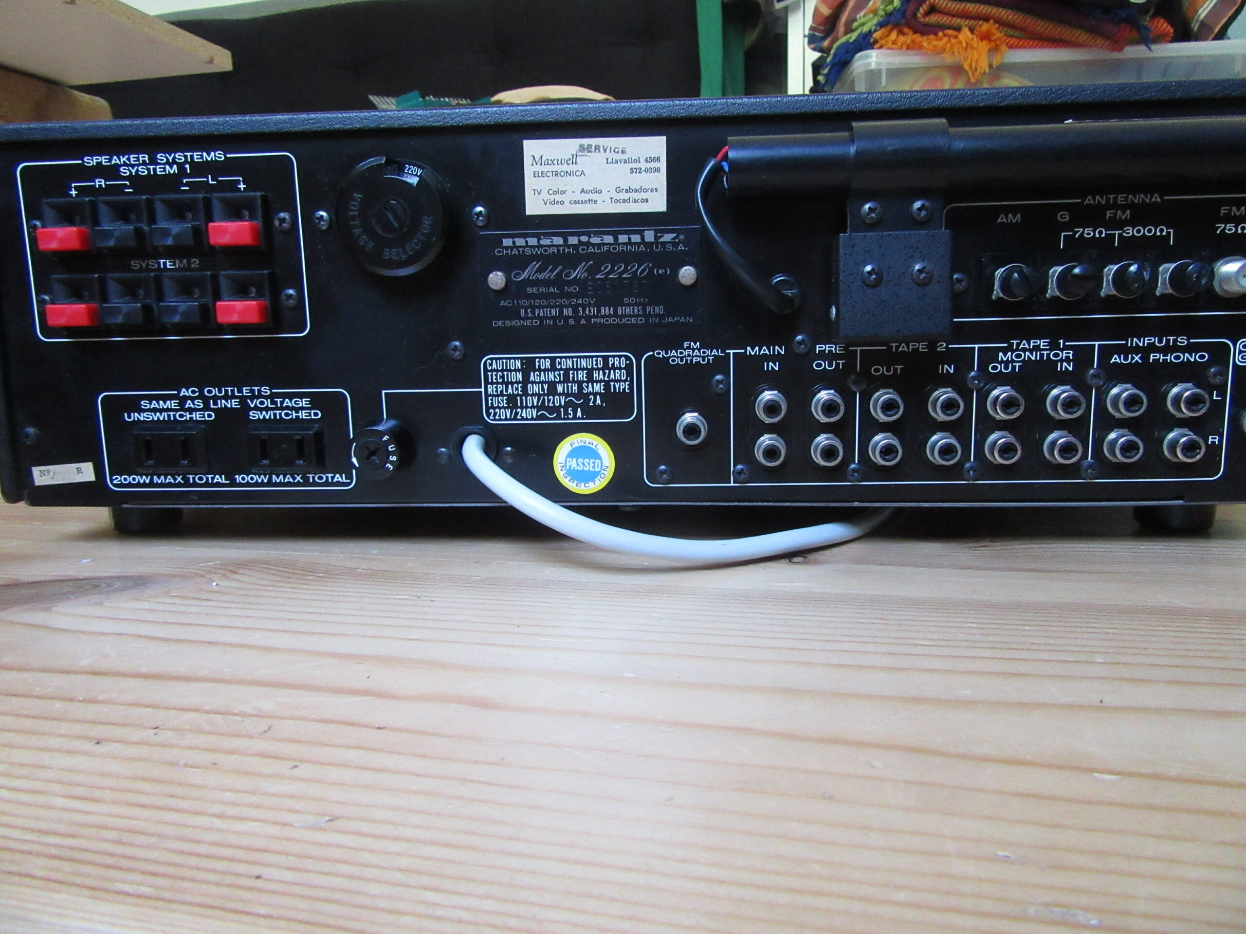
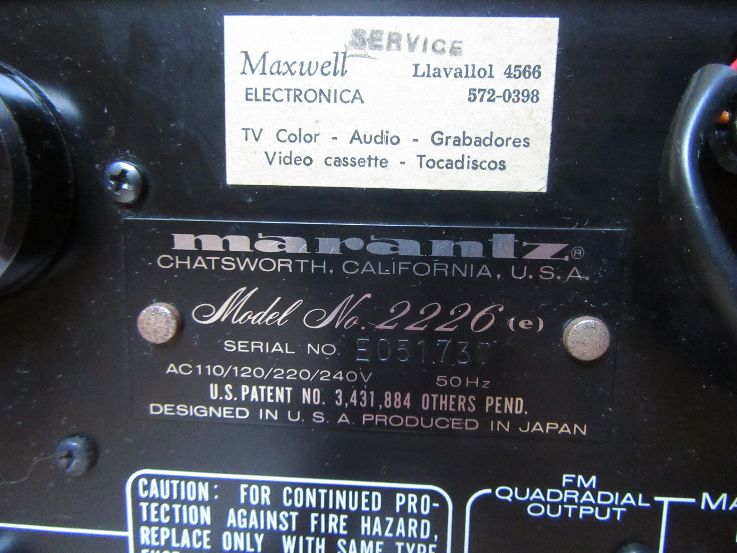
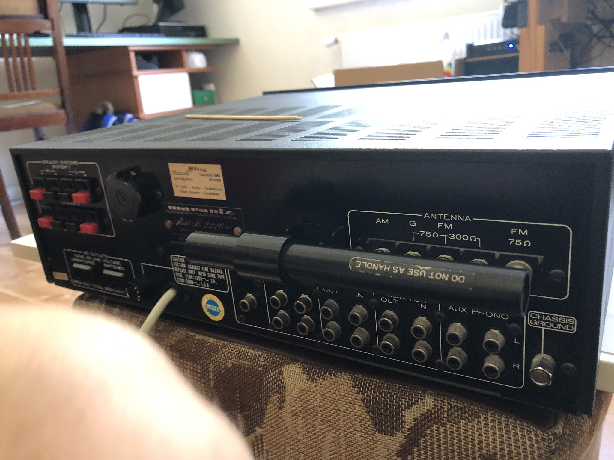
There was also a bit of family history involved, as the unit traveled with my girlfriend’s family to Buenos Aires in the late 70s. After a few years there and at least one repair, the receiver came back to Germany as part of the family. A sticker of the service workshop “Maxwell Electronica” still testifies to the stay in Argentina. At least Google Maps still finds the company at the given address.
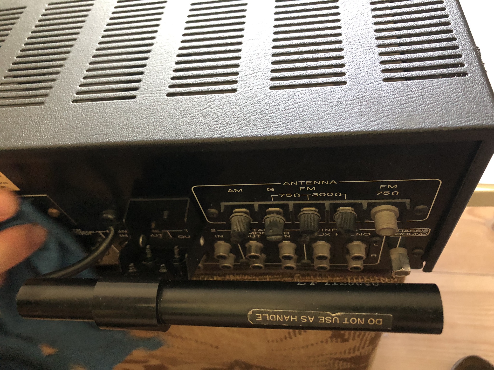
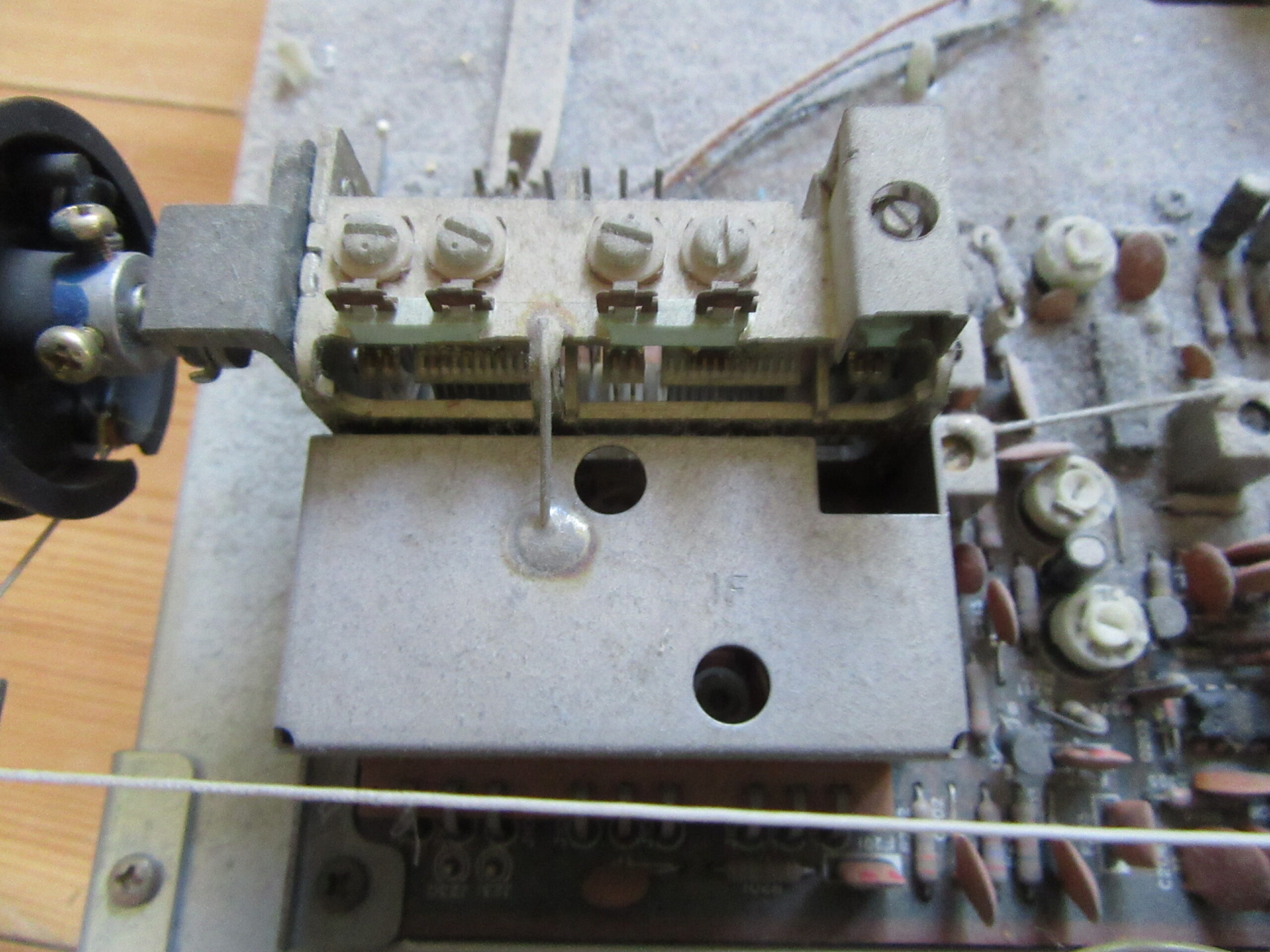
The workshop apparently repaired the scale lighting and adapted instead of the pilot bulbs incandescent lamps with E10 base. They had too much power and the plastic parts got too warm. Fortunately, the resulting discoloration can only be seen from behind.
But now the photos, without comment. First the initial state and part two with pictures after the repair.
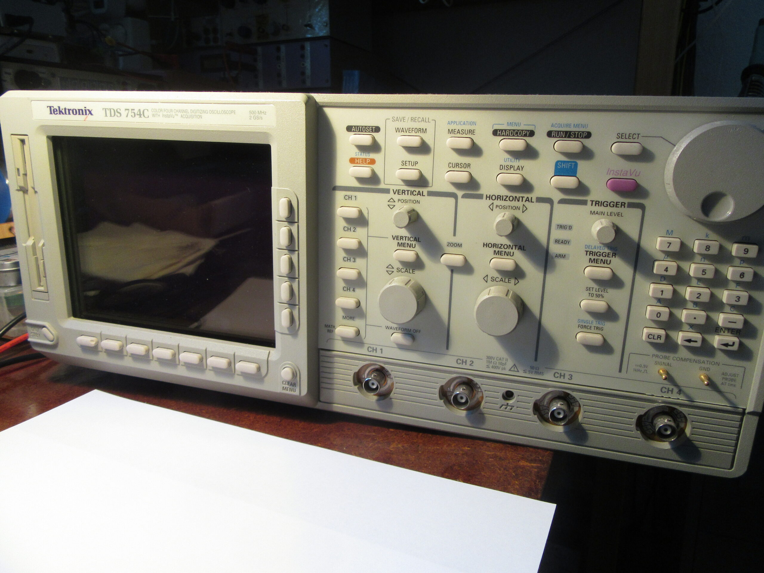
Finally there was a day off at the weekend. This time I wanted to use it to perform a maintenance on my Tektronix TDS754C digital oscilloscope that had been pending for years. The plan was to replace the two ICs from “Dallas Semiconductor” with integrated lithium battery. And that before they fail and lose all data. After 24 years. There is no more time to waste.
TDS754C Front view
Preparation
The preparation for this maintenance started years ago and took a long time, as it is with hobbies. Two things I had to do in advance:
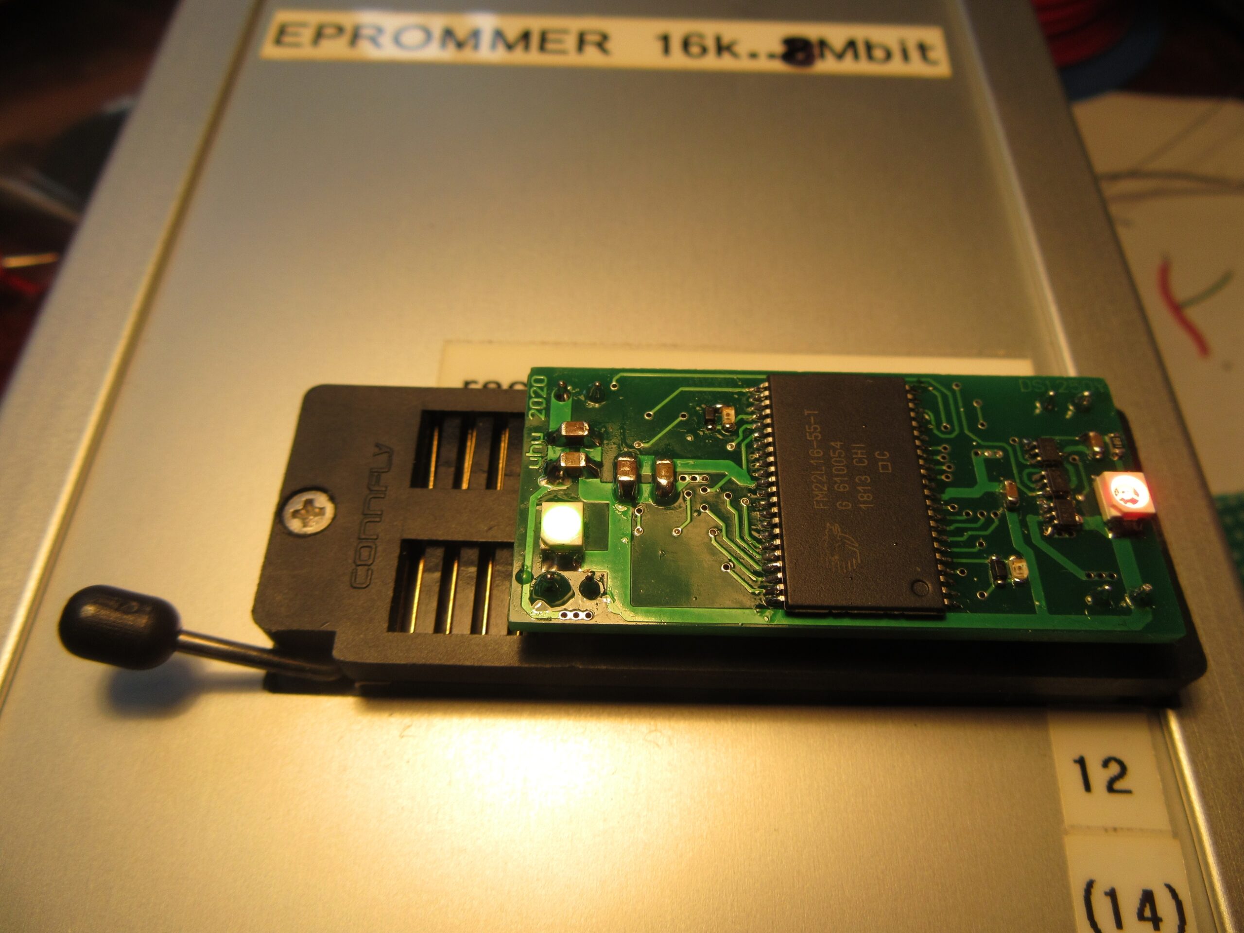
Upgrade my homebrew programmer to 4MBit and make it able to read and write FRAM and NVRAM chip types.
Building a replacement for DS1250Y or DS1650Y chips.
I had already finished the extension of my programmer in 2018. I was able to check off the second item this spring and have described it in detail here.
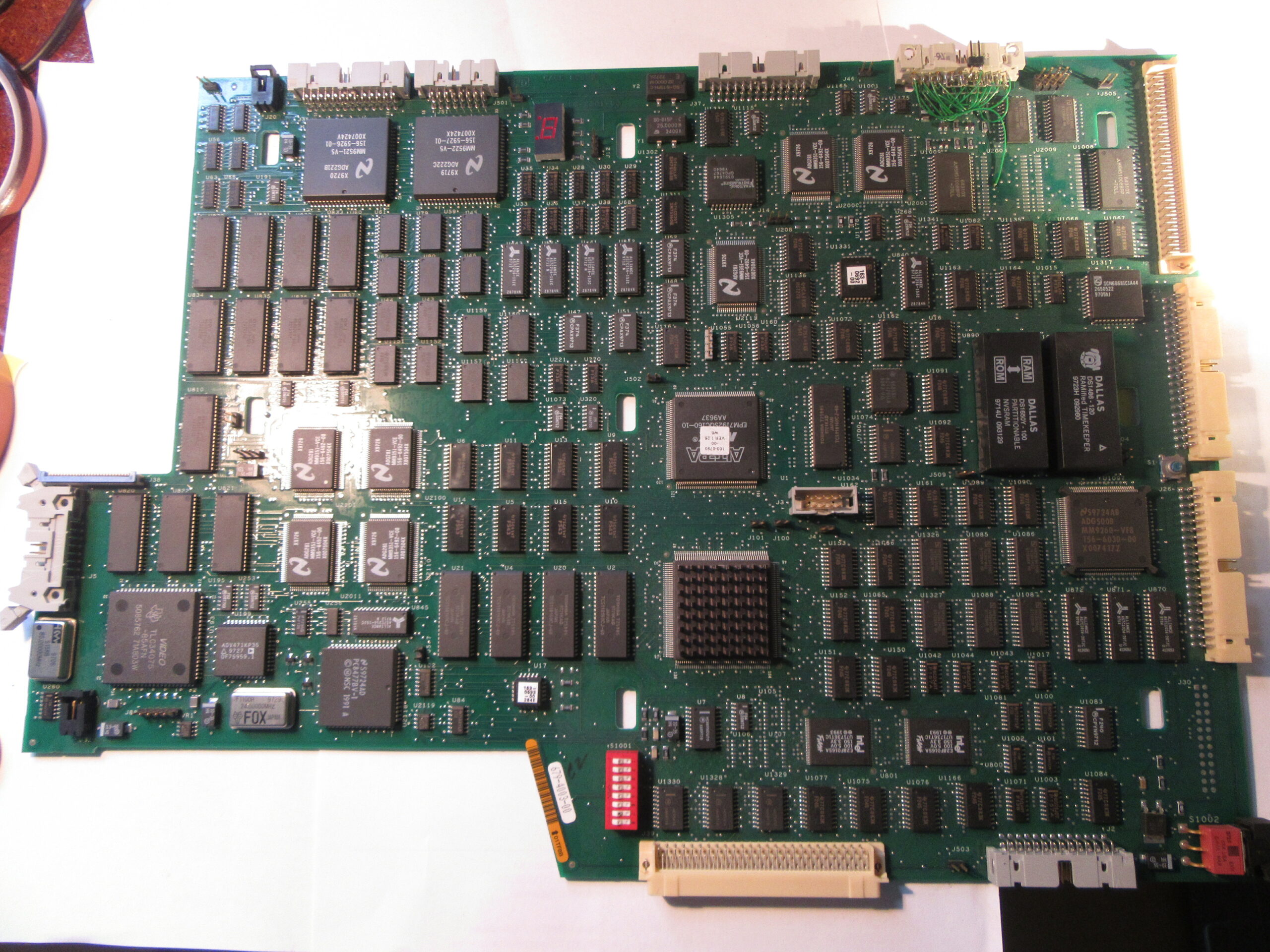
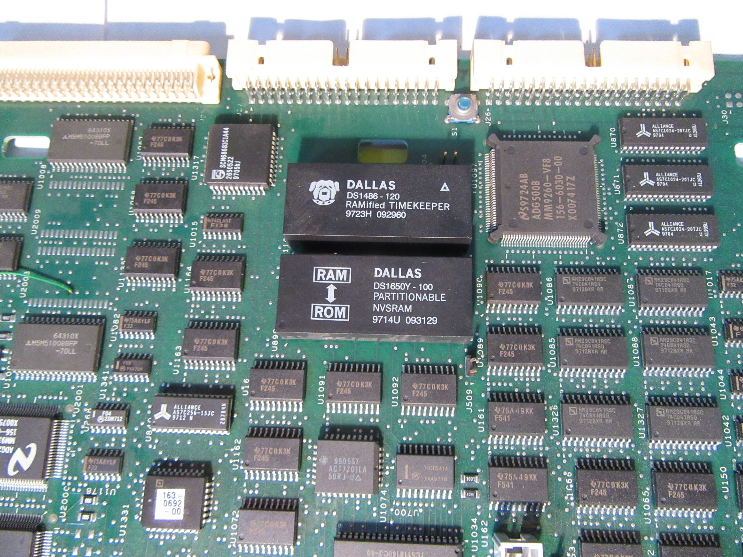
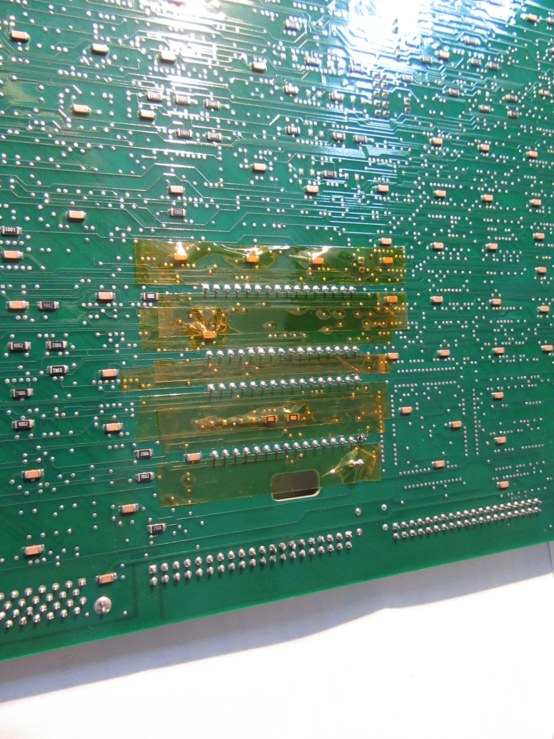
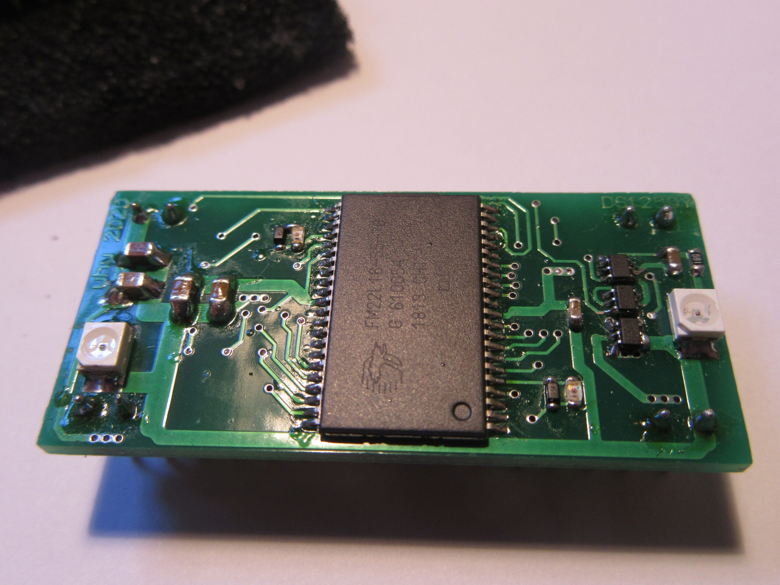
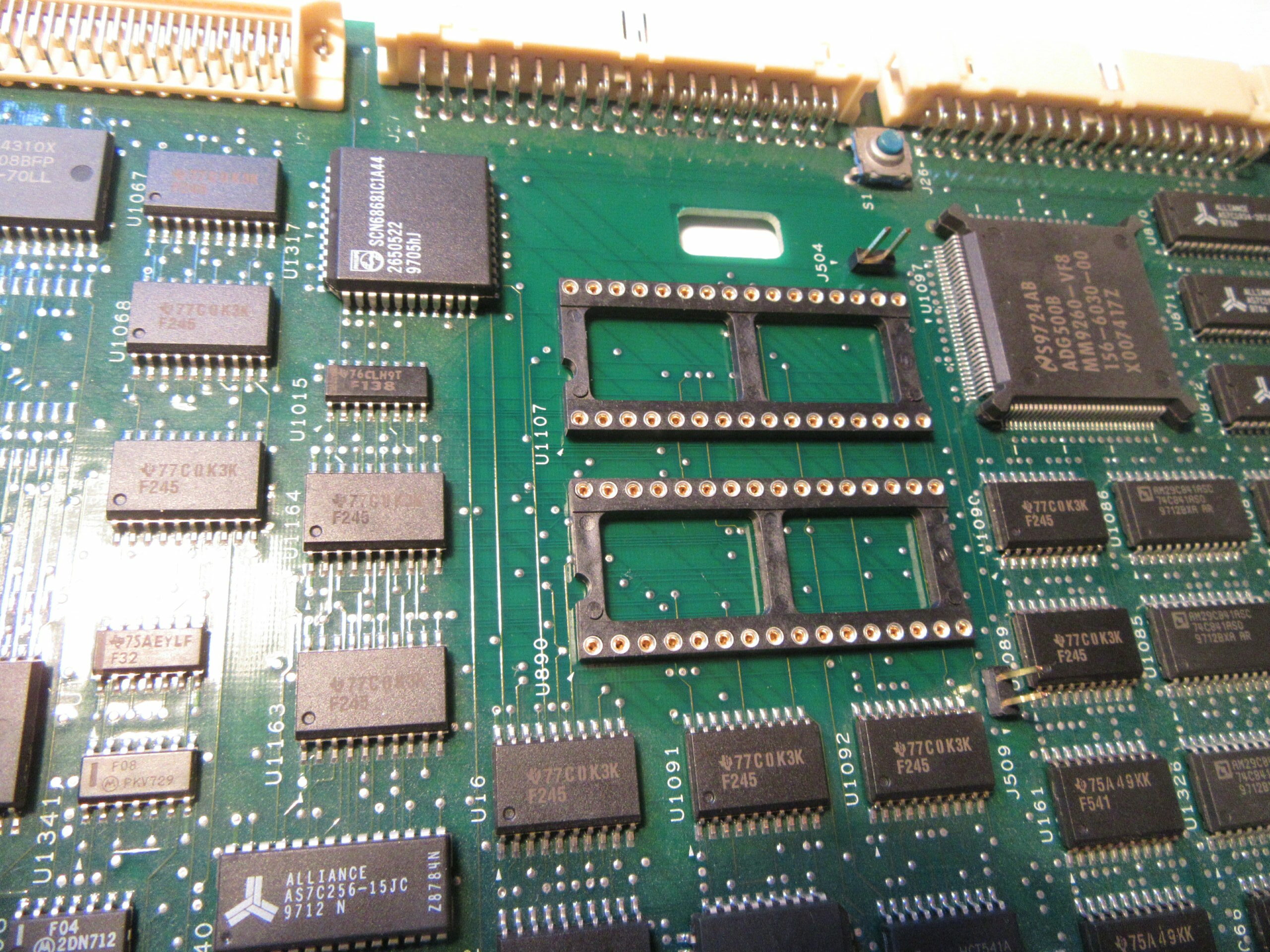
There are two of these ticking time bombs installed in the device, Dallas chips with integrated Lithium battery. I also described the problem with these components in more detail in this article. Specifically, it is a DS1486 RTC+1MBit NVRAM and a DS1650Y 4MBit NVRAM, both of which are soldered onto the CPU board.
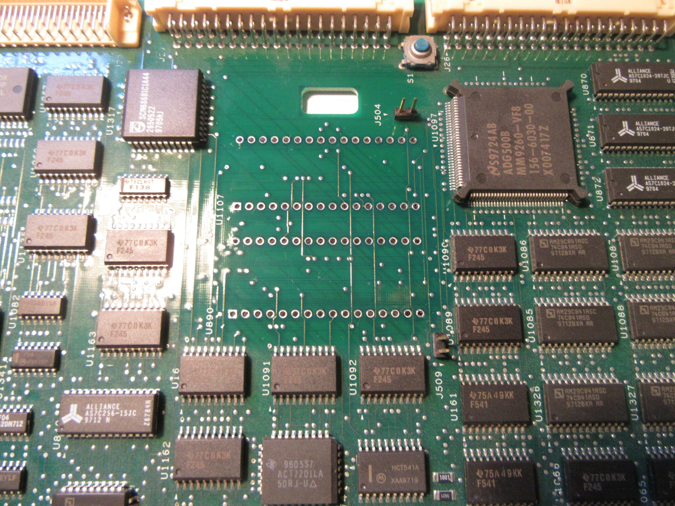
CPU boardCPU board close up Dallas chips
In the case of the oscilloscope here, a failure of the two ICs would mean that calibration data and information about enabled additional functions would be lost. After all, the built-in batteries lasted from 1997 to 2021. With ten years of guaranteed life, that’s almost two and a half times the time.
Data backup
First, it’s a good idea to make a backup of the NVRAM contents. The device has a built-in 1.44MB HD floppy drive. Fortunately, someone wrote some scripts and posted them here that allow you to back up the NVRAM to a floppy.
For me the whole thing worked flawlessly on the first try. I used the tool “tdsNvramFloppyDumper”. Later I used the programmer to write the data to the replacement chips.
Desoldering
Now it was time to desolder the old parts. The oscilloscope is built very service friendly. To remove the CPU board, no instructions are necessary in my opinion. The desoldering itself I always do with this somewhat larger manual desoldering pump and a normal electronic soldering iron.
Surrounding area masked with tape
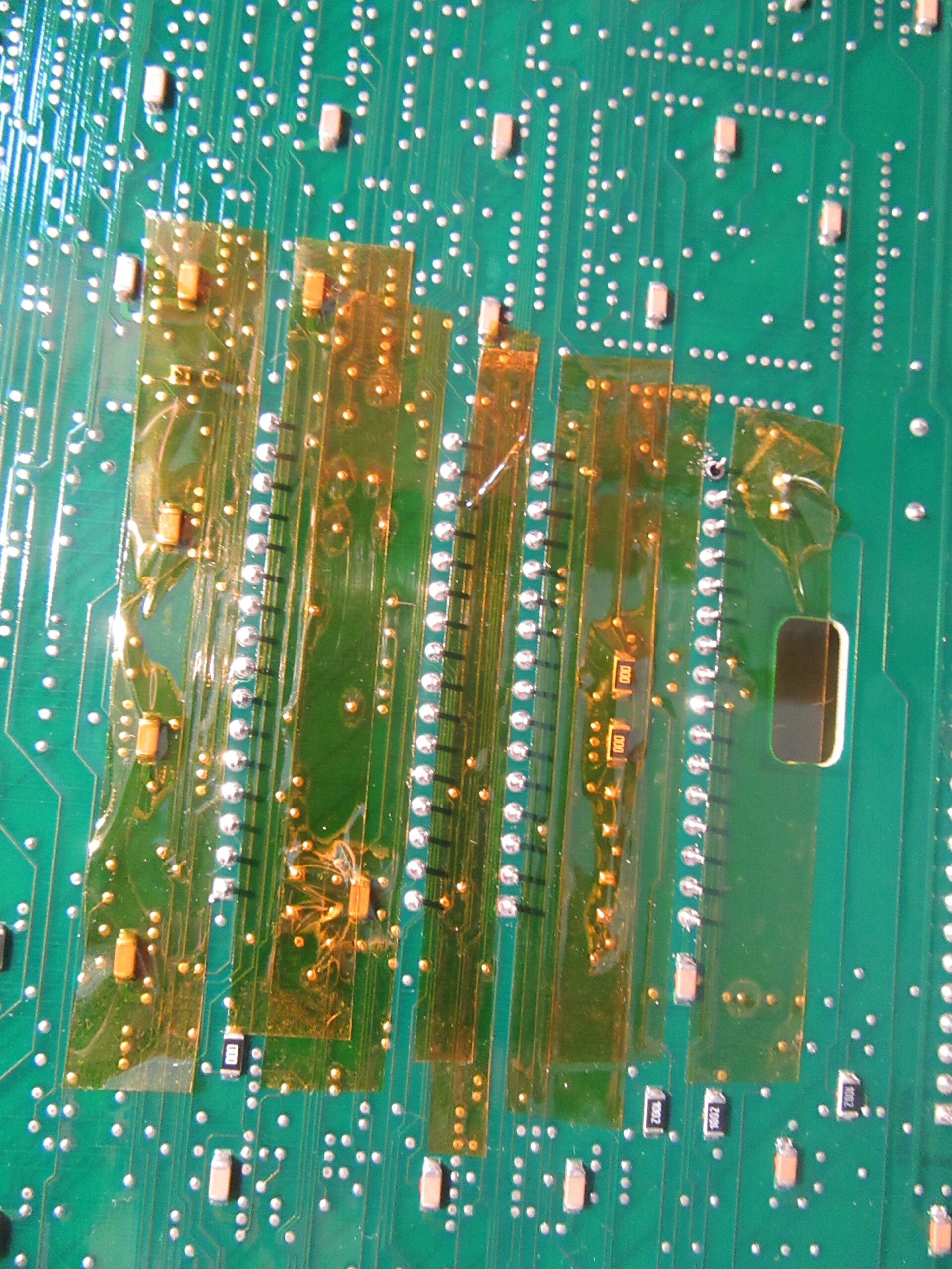
It is important to protect adjacent thin conductors with Kapton tape. The recoil of the pump throws the soldering tip a little bit away when triggering. This occasionally destroys thin conductors next to the solder pads. The tape reliably prevents this in my experience. The desoldering worked fine, I also had only one attempt.
Close up Kapton tape for protectionBoth Dallas ICs desolderedFreed solder pads close up
Exchange parts
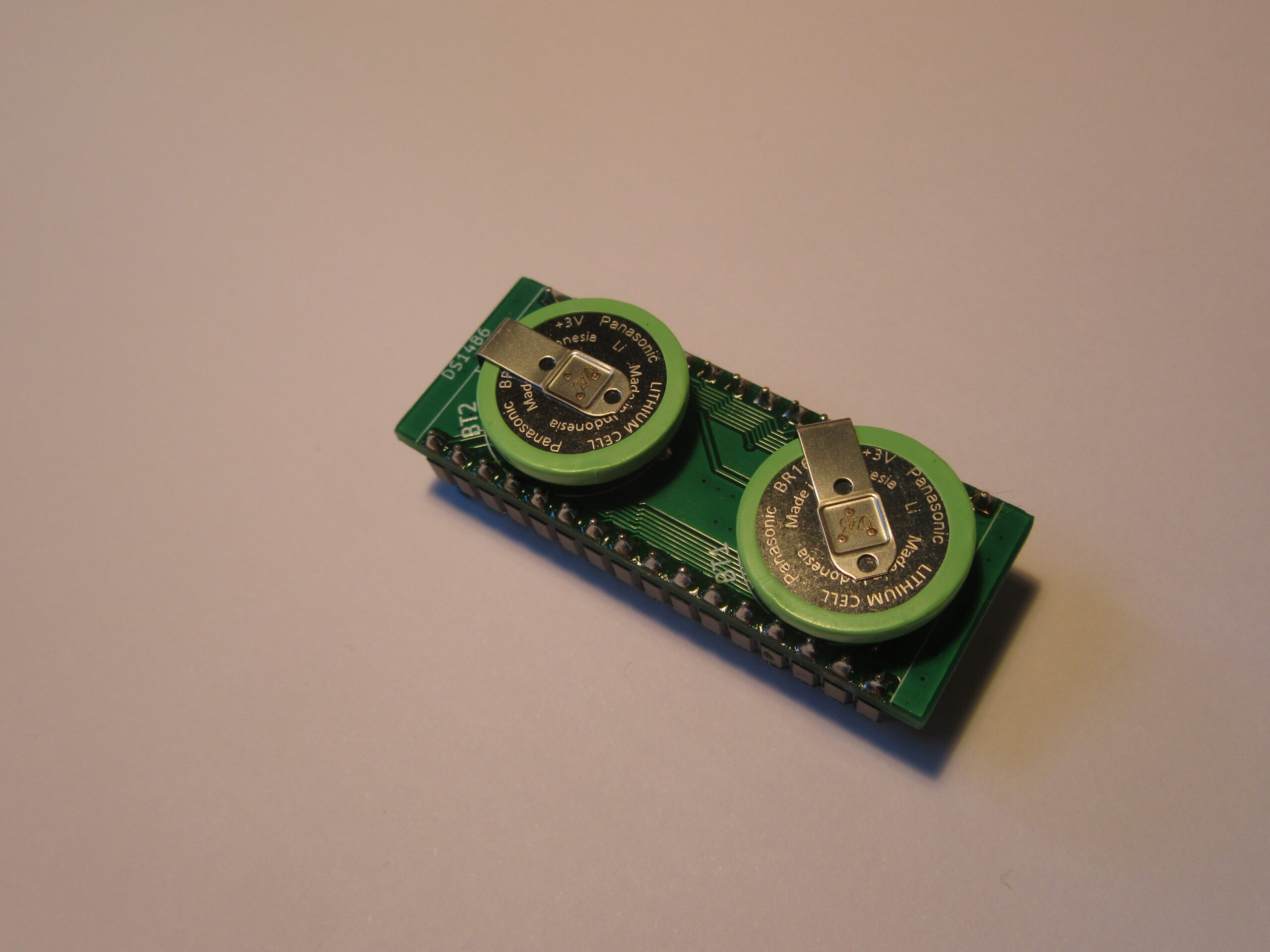
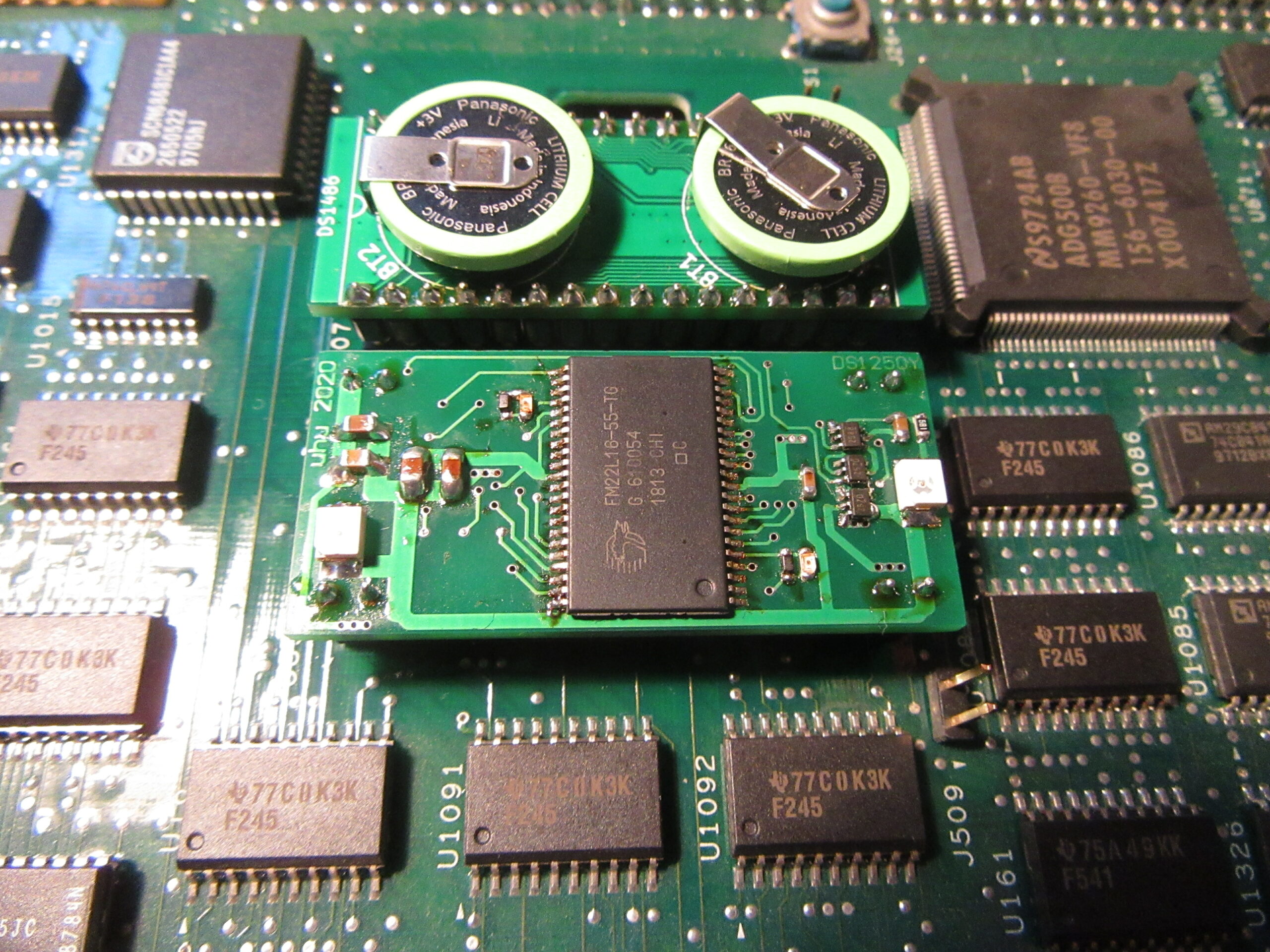
DS1486
The RTC is the more difficult part. I was lucky and found a ready-to-use rebuild instructions on the net as well as a remaining stock seller from China, who sells the obsolete DS1384G, which is necessary for the replacement. Nevertheless, be careful with the purchase, also from this IC all kinds of fakes are traded.
Rebuilding the small module was easy. During testing I learned that both batteries must be connected for the RTC to work. At first I had tested this only with the primary battery.
DS1486 Replacement module with batteriesDS1384G hidden under one of the batteriesDS1486 Replacement module from below
Another thing worth mentioning is the choice of batteries. There are six different common lithium battery technologies and some exotic. All have different voltages, advantages and disadvantages. In this case here it is important that the self-discharge is low and the capacity is high. This guarantees a long service life. The type “BR1632A/HAN” from Panasonic used here is a lithium carbon monofluoride battery, which meets these requirements.
DS1650Y
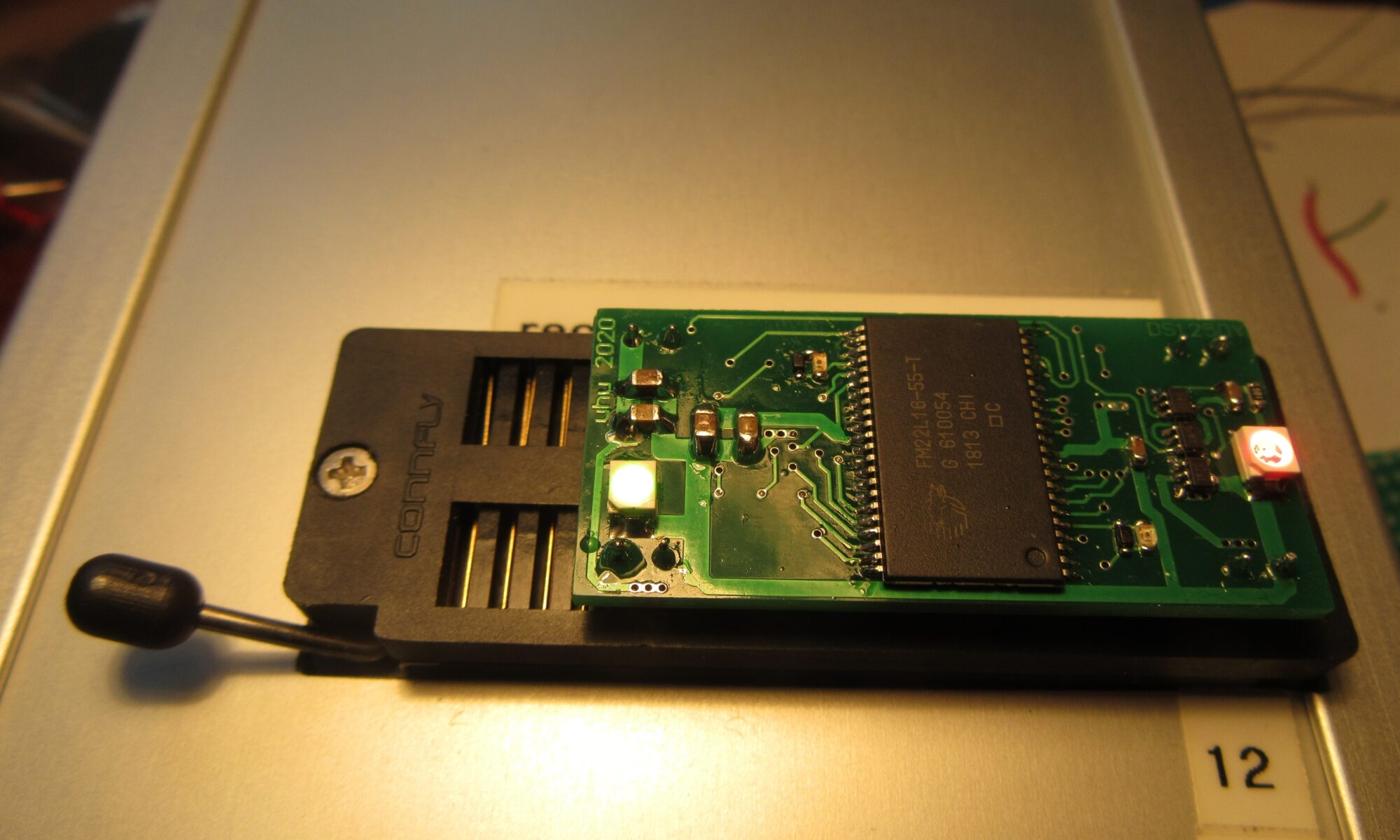
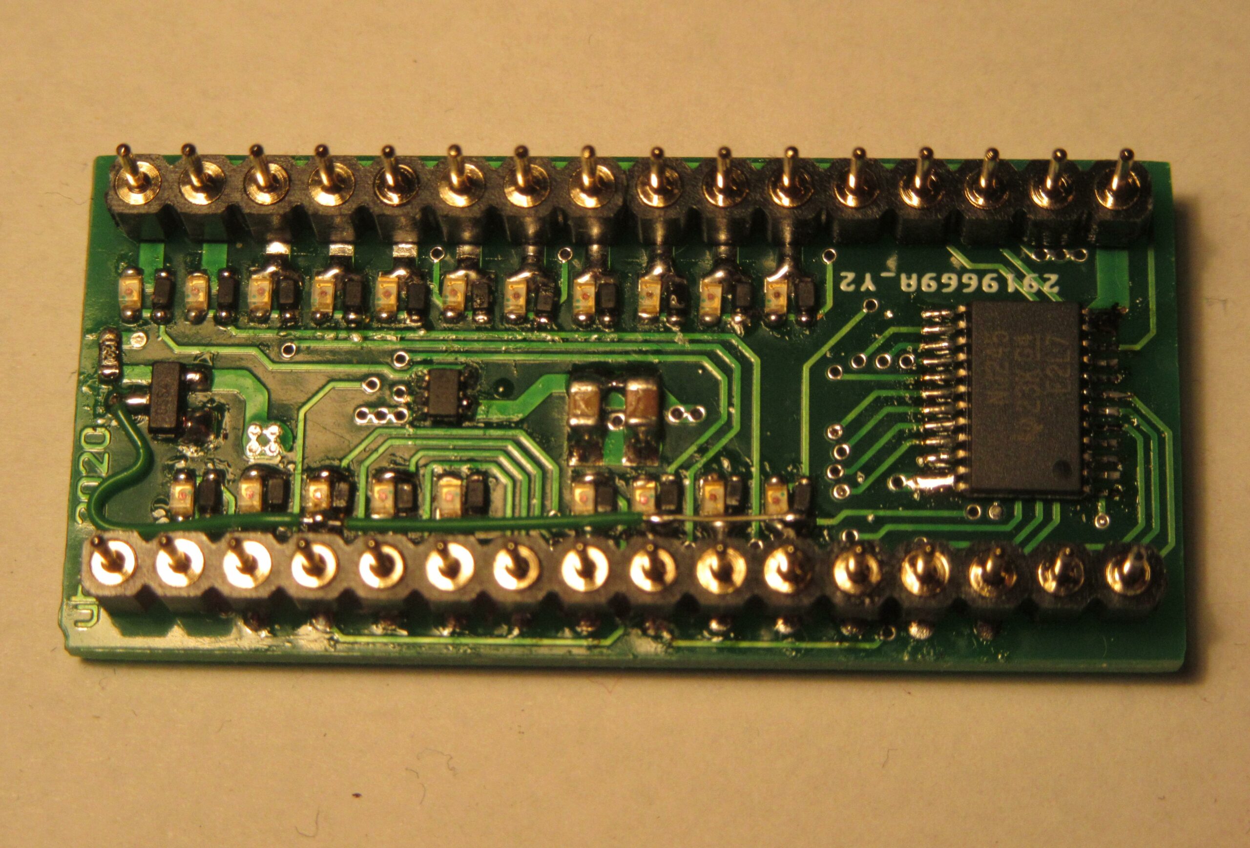
The replacement based on a FRAM for the 4MBit NVRAM DS1650Y I developed myself at the beginning of this year. It is described in detail in the article. In the TDS754C a DS1650Y is installed, but the write protection feature of the component is not used. The replacement with the FRAM module is therefore possible.
DS1650Y FRAM replacement module
Installation
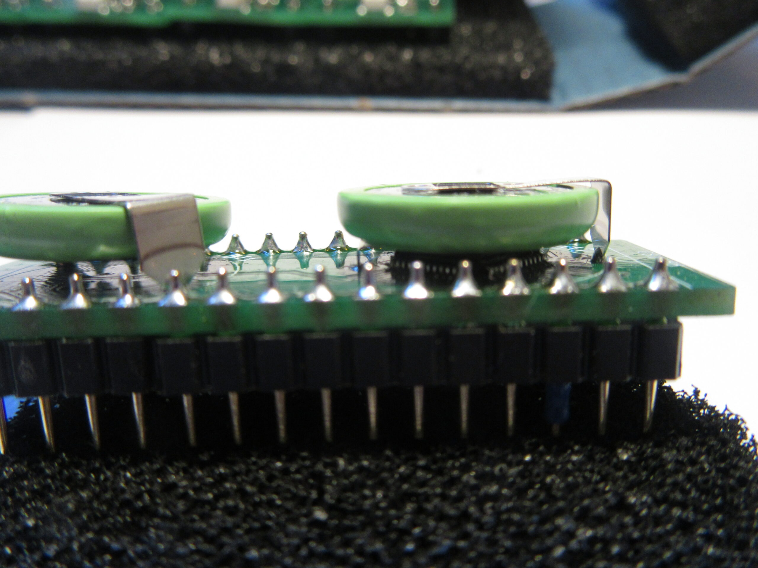
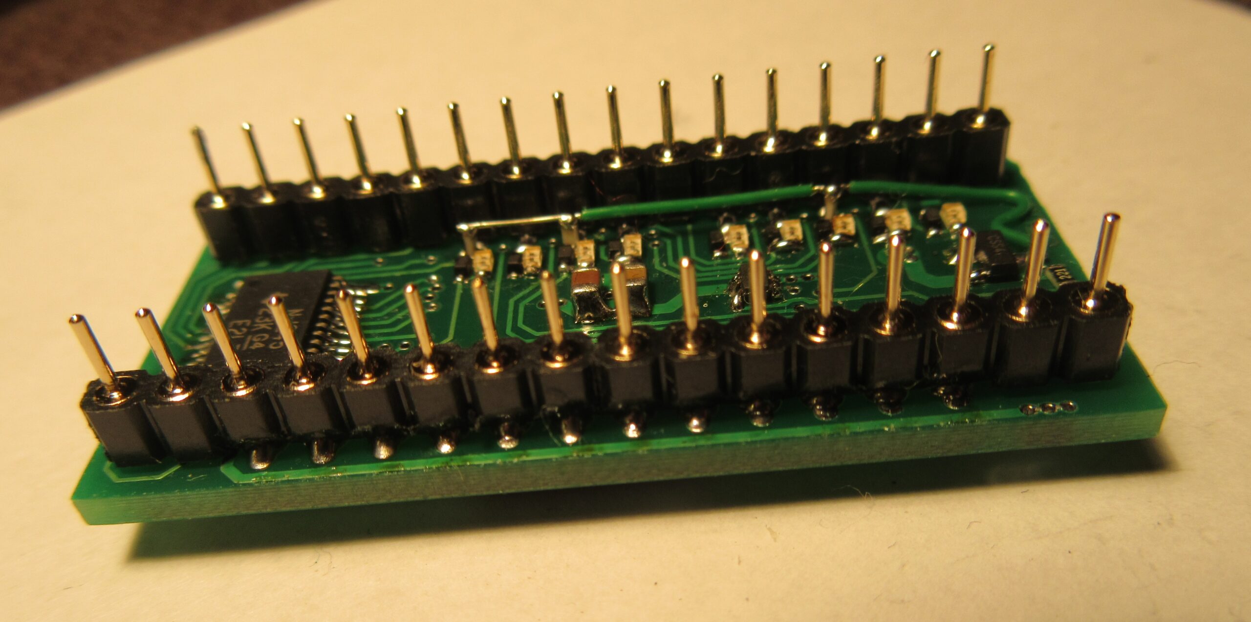
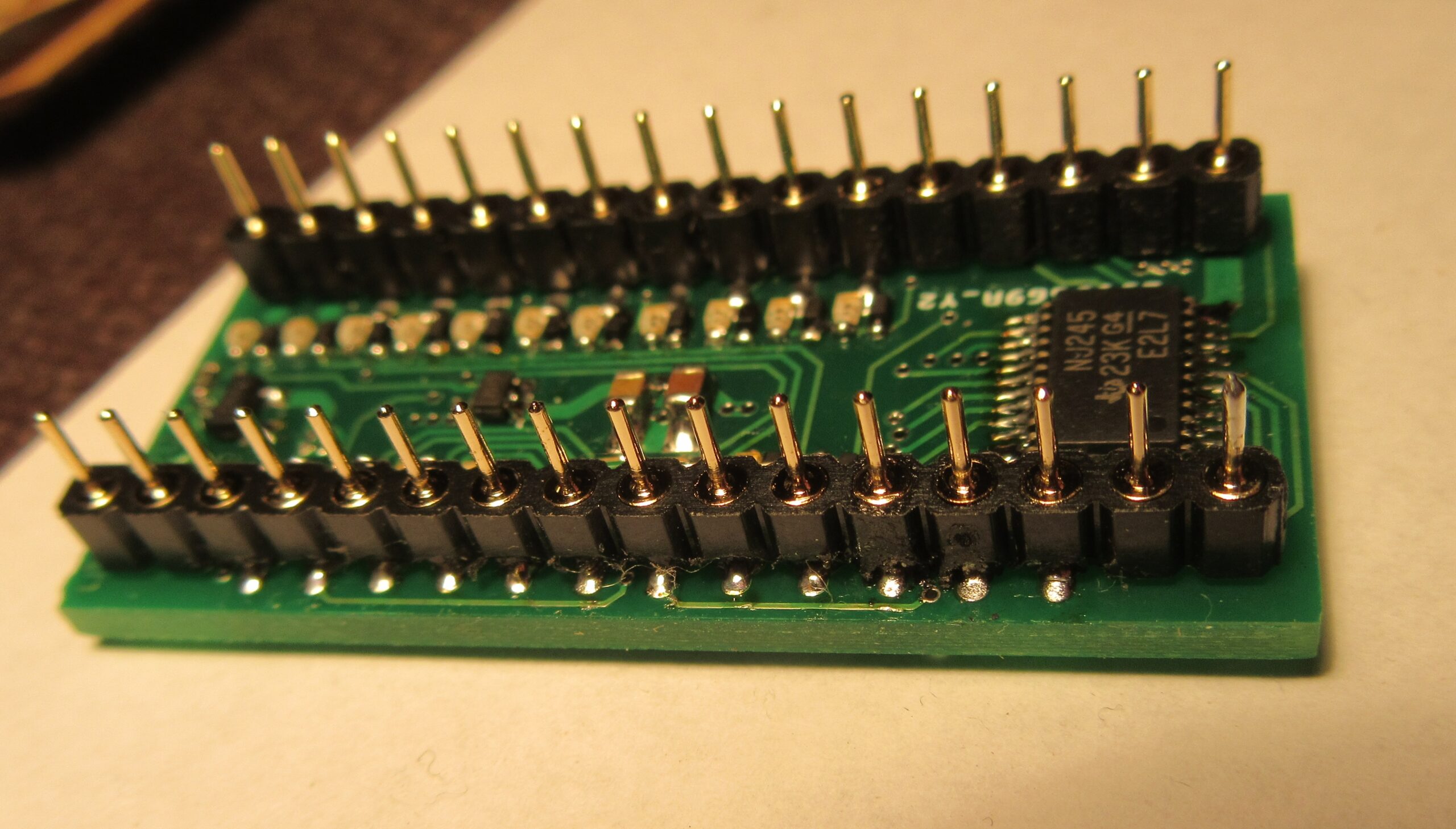
The new components are conveniently socketed. This makes it easy to remove the modules to replace the batteries, for example. Besides, it was uncertain whether the exchange would work. In case of problems, I could have simply put the two soldered out parts back into the socket.
As sockets I use some with a low profile. The contacts are partially recessed in the board. This makes the replacement part with socket only slightly higher than the original.
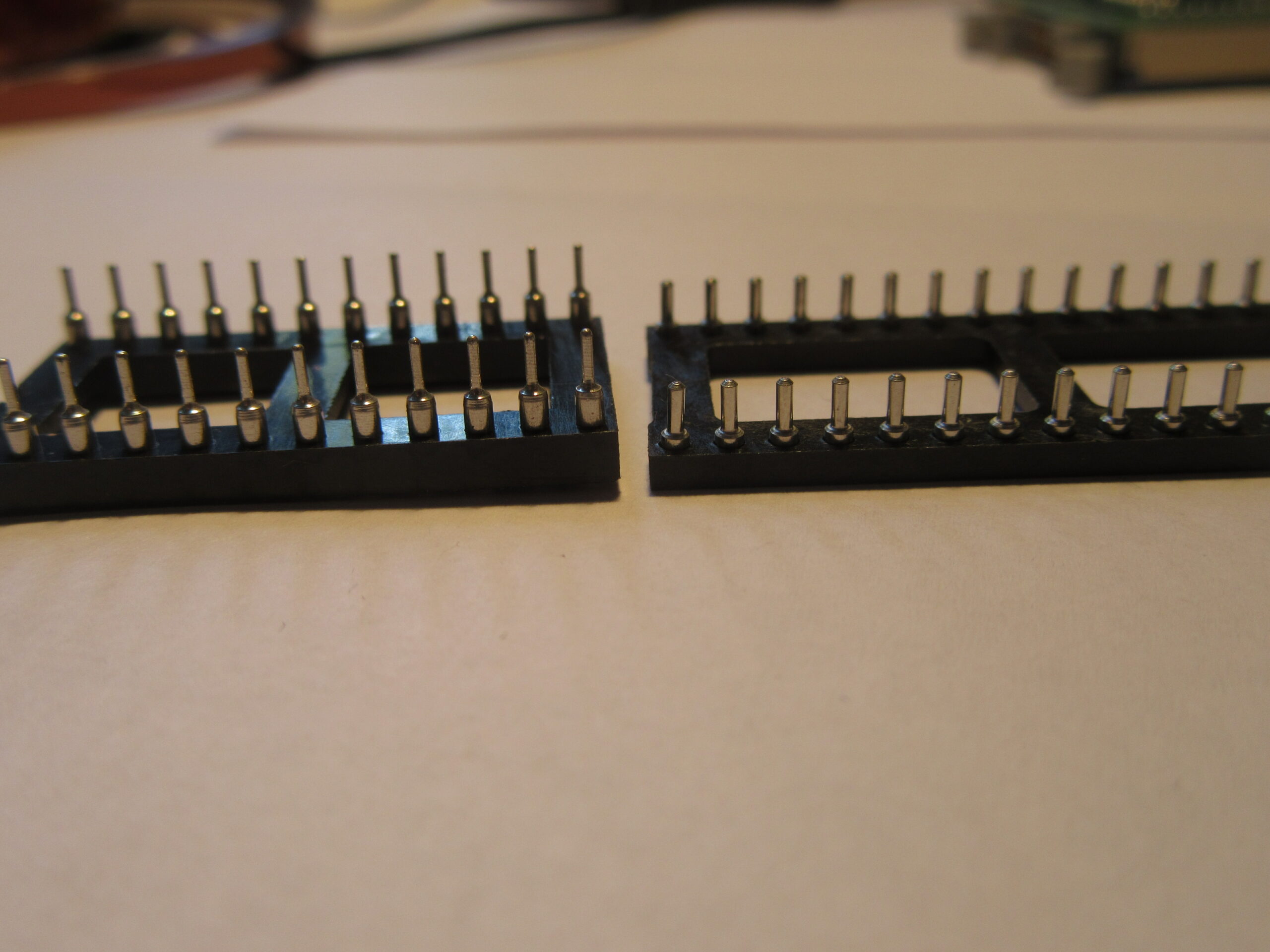
Left standard socket, right low-profile version
The two sockets were quickly soldered in place. It was annoying that the pin headers of the two replacement modules were a bit too thick. Thus they do not fit completely into the socket and are relatively difficult to insert and remove. I should have read the data sheets of the mechanical components beforehand.
Socket ready solderedSpare modules equipped
Putting into operation
First, the device reported an NVRAM CRC error after power-on. Maybe the memory was written during the backup which leads to an invalid checksum. The attempt to restore the backup with the above linked “tdsNvramFloppyTools” was successful. The device now starts again as usual and at least the two replaced parts will do their job for many more years.
This project is not very big but still something special. On the one hand it is part of a restoration which has been prepared for years. On the other hand it seems that nobody has come up with the idea to replace a 5V NVRAM with a 3.3V FRAM or to publish it.
Problem components NVRAM
If you want to keep old devices for a long time, you will always come across chips with integrated lithium battery from “Dallas Semiconductor”, which was bought by “Maxim Integrated” in 2001, which in turn was bought by “Analog Devices” in 2021. These are mostly NVRAMs (non-volatile RAM) or RTCs (real-time clocks) with NVRAM. The battery integrated in the chip package enables the data in the RAM to be retained even after the operating voltage is switched off and the RTC continues to run. An NVRAM controller, which is also integrated, takes care of switching between battery and operating voltage as well as data protection when switching on and off.
Basically, this is a very practical solution, since one can use a single component instead of a whole circuit including battery. However, it is fatal when the built-in battery is exhausted after about 20 years. Almost always the whole device is no longer functional. The components are of course no longer produced. Also the remaining stock traded on the Internet is either already too old or even more often faked. I have bought two fakes myself. Thus, replacement with the original part is not an option.
Soldered NVRAM and RTC (Tektronix TDS754C CPU Board)
Replacement options
The replacement of RTC and NVRAM differs significantly.
The NVRAM can be replaced by a corresponding SRAM with NVRAM controller and battery. Some examples can be found on the net.
Another variant is the replacement by FRAM, a memory which can be written arbitrarily like RAM, but which keeps the content even without operating voltage. There are also examples with the FRAM types FM16(W)08 and FM18(W)08 with 64kBit and 256kBit size respectively. The charm of this solution is that no battery is necessary and thus the memory remains maintenance-free. Unfortunately, the two mentioned FRAM types are pin-compatible with the Dallas NVRAMs, but they are controlled somewhat differently. Thus the exchange unfortunately does not work in all devices.
An RTC cannot be replaced so easily. The RTC maps the time to a memory area that is accessed like “normal” RAM. The chip has to keep the required timing exactly. This can only be ensured by using dual-port RAM. However, I have not found suitable circuits. This would be a small project for the future. Currently, there is only the possibility to mechanically drill out an old RTC and connect a new lithium battery from the outside. Or you can use a compatible RTC chip, which is still available as residual stock. As far as I know this is only possible for a DS1486, which is replaced by a DS1386G incl. RAM and battery.
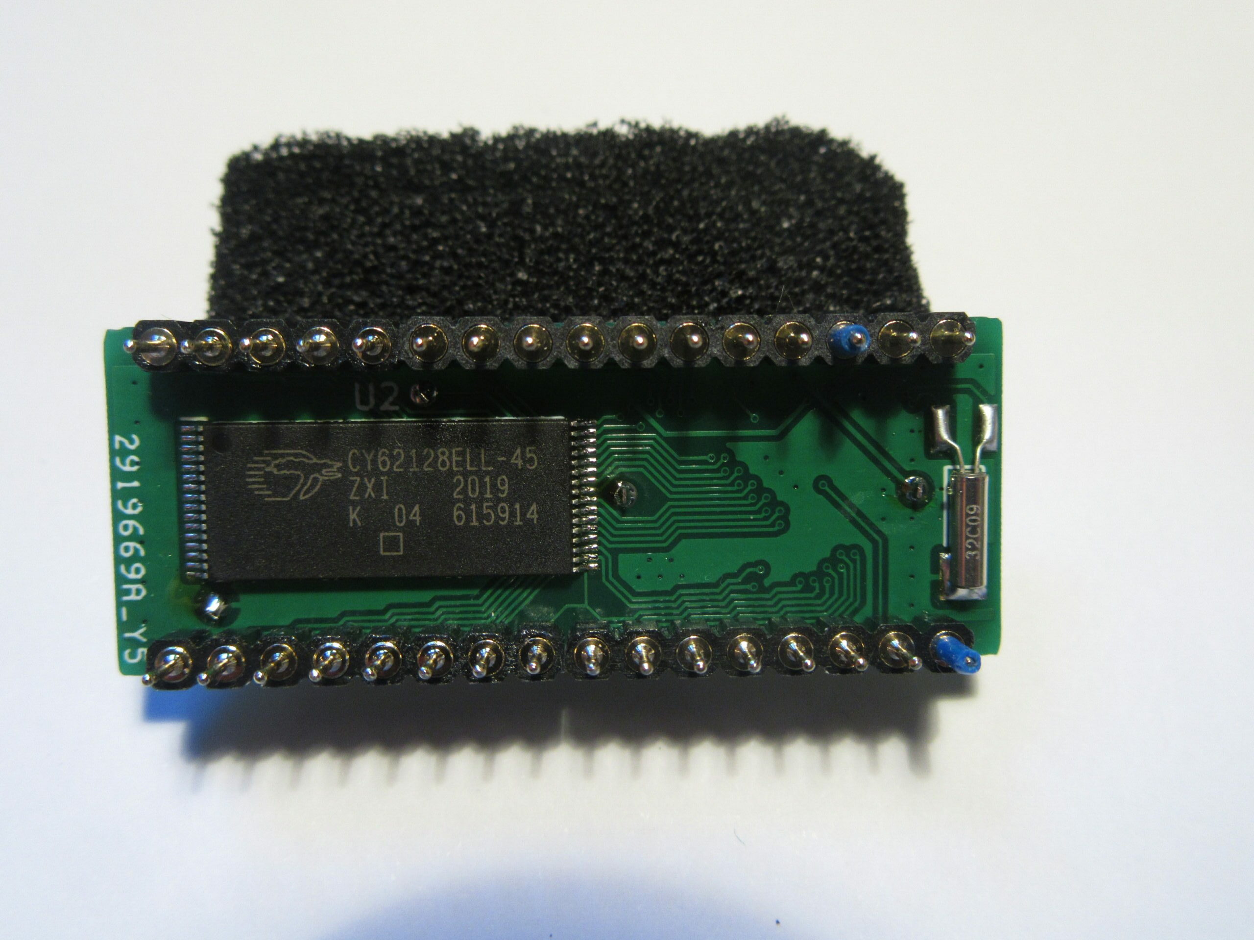
DS1250Y/DS1650Y FRAM Replacement
Now to the corpus delicti. The DS1250Y component from “Dallas Semiconductor” is a 4MBit NVRAM. The pin-compatible DS1650Y variant also has the option of write-protecting individual memory areas via software. Thus the DS1650Y can replace the DS1250Y. The other way around, this doesn’t work in every case, but only when the software doesn’t use the write protection feature or doesn’t depend on it.
A short component search for parallel 4MBit FRAM brings only one product to light, the FM22L16-55-TG. Unfortunately, it works with a maximum of 3.3V and has 16 bit data width in contrast to 5V and 8 bit on the DS1250Y.
So there are still some parts missing to adapt the FM22L16: Some logic, level shifter, a voltage regulator and some brain power. Difficult in the design was also that the whole circuit has to fit on a board with the size of the original part.
Circuit
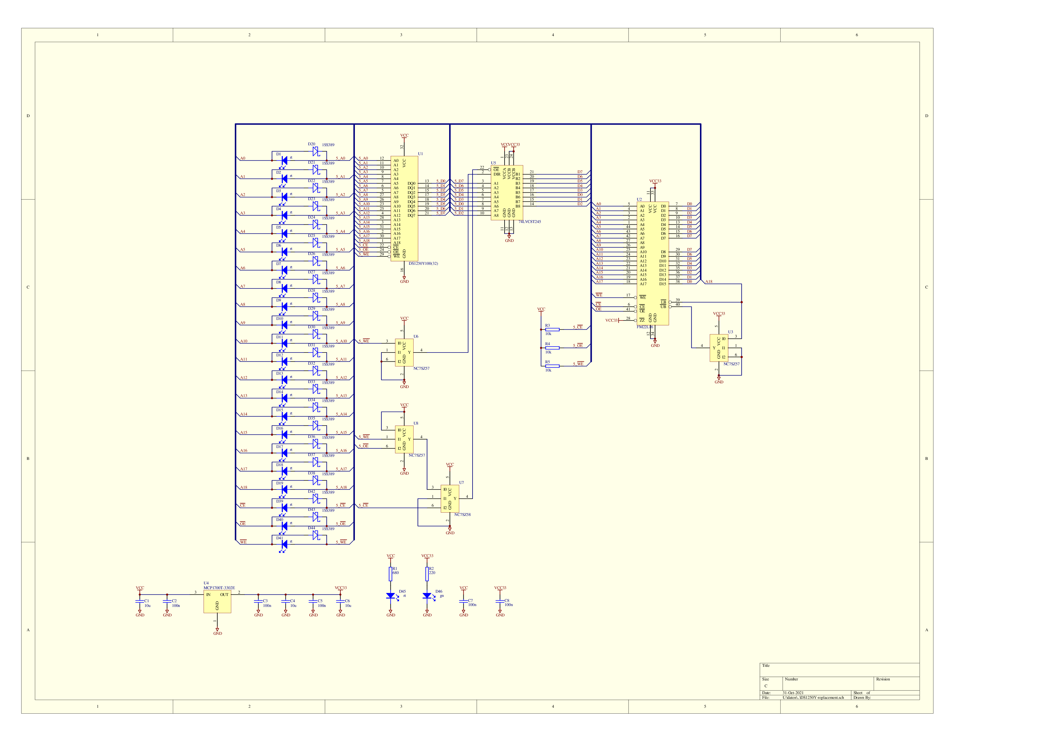
After a couple of days of reading and understanding data sheets and drawing schematics, the circuit was ready.
Circuit diagram
I used a bidirectional level shifter 74LVC8T245 for the data bus, a MCP1700T-3302E low dropout voltage regulator for the 3.3V power supply, a couple of universal single gates for the control logic and Schottky diodes and LEDs for the unidirectional level shifters of the address and control lines.
In the first version I had forgotten the pull-up resistors R3 to R5 which caused the data to be changed when the device was removed from the programmer. Otherwise, the circuit works flawlessly and easily meets the timing requirements of the original.
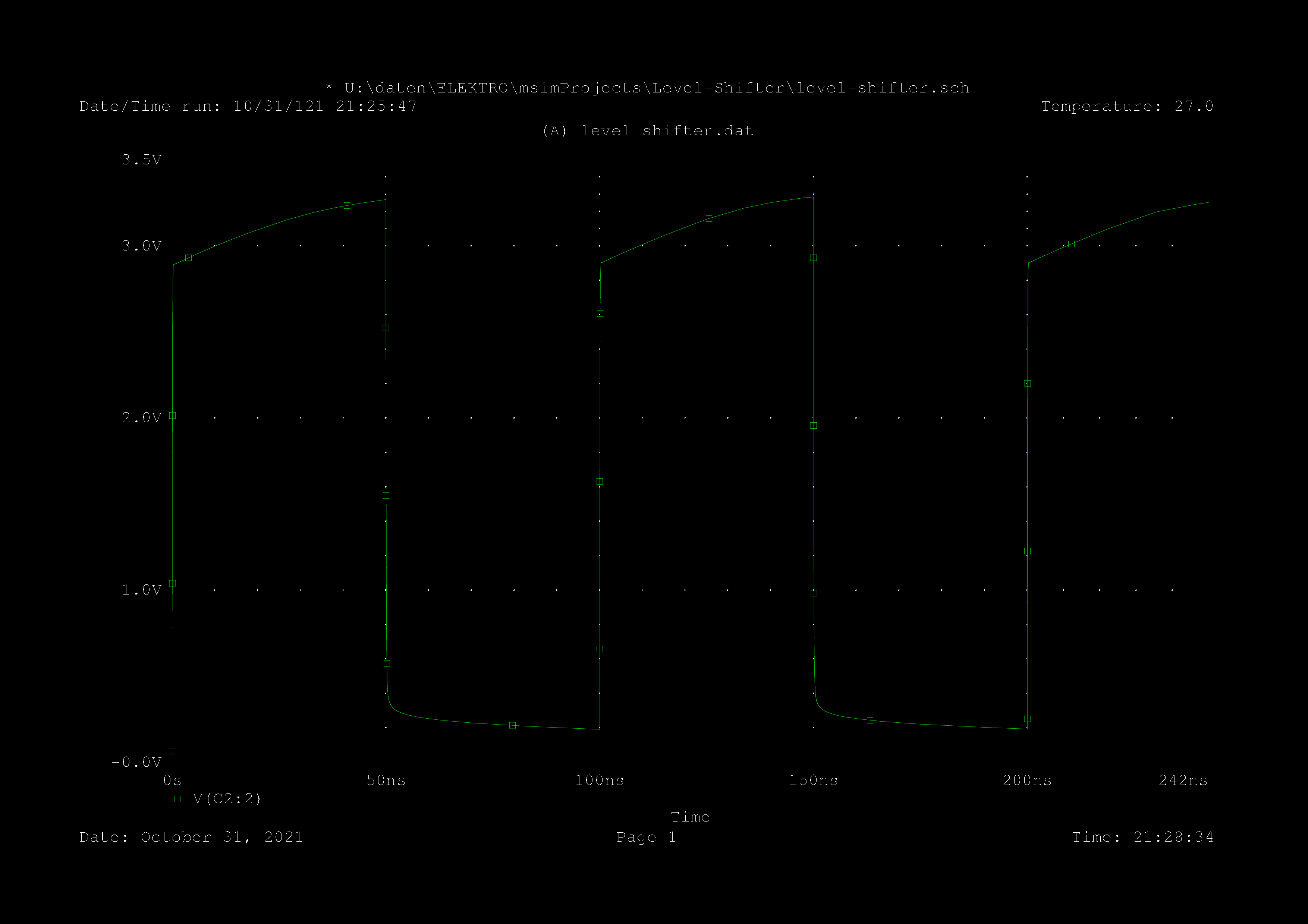
The unidirectional level shifters with a Schottky diode plus LED are still special and grown on my crap. I simulated the circuit and found that this simple way works safely and quickly.
Simulation level shifter for address and control lines
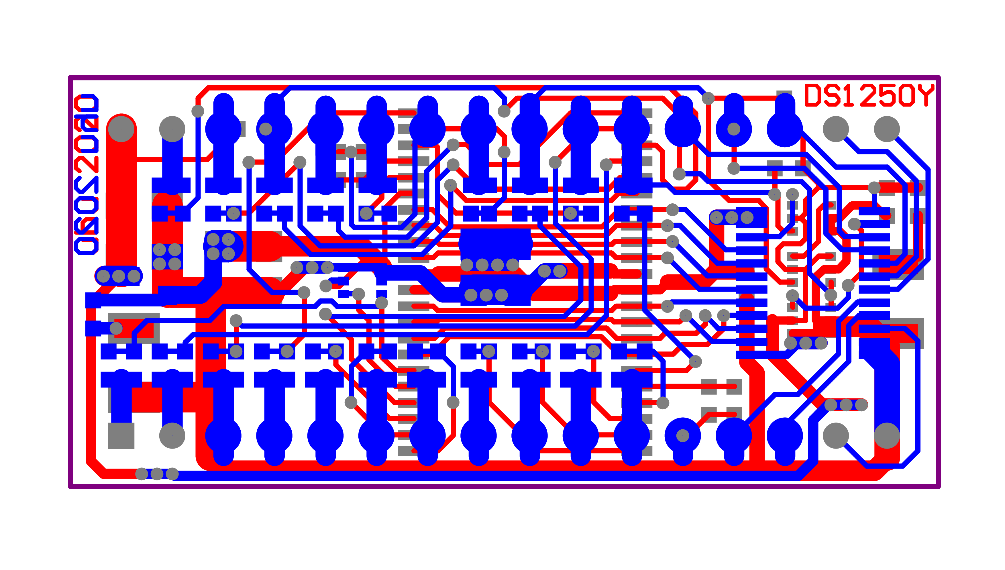
The circuit is placed on a double-sided PCB, which is about 1mm wider than the original component. In most devices, however, there is enough space for it.
Board layout
Gerber Files for private reorder are located here. Usually I order at JLCPCB. There you can simply upload the zip for ordering. The bill of materials and the assembly plan are here.
The rest follows as a short picture story:
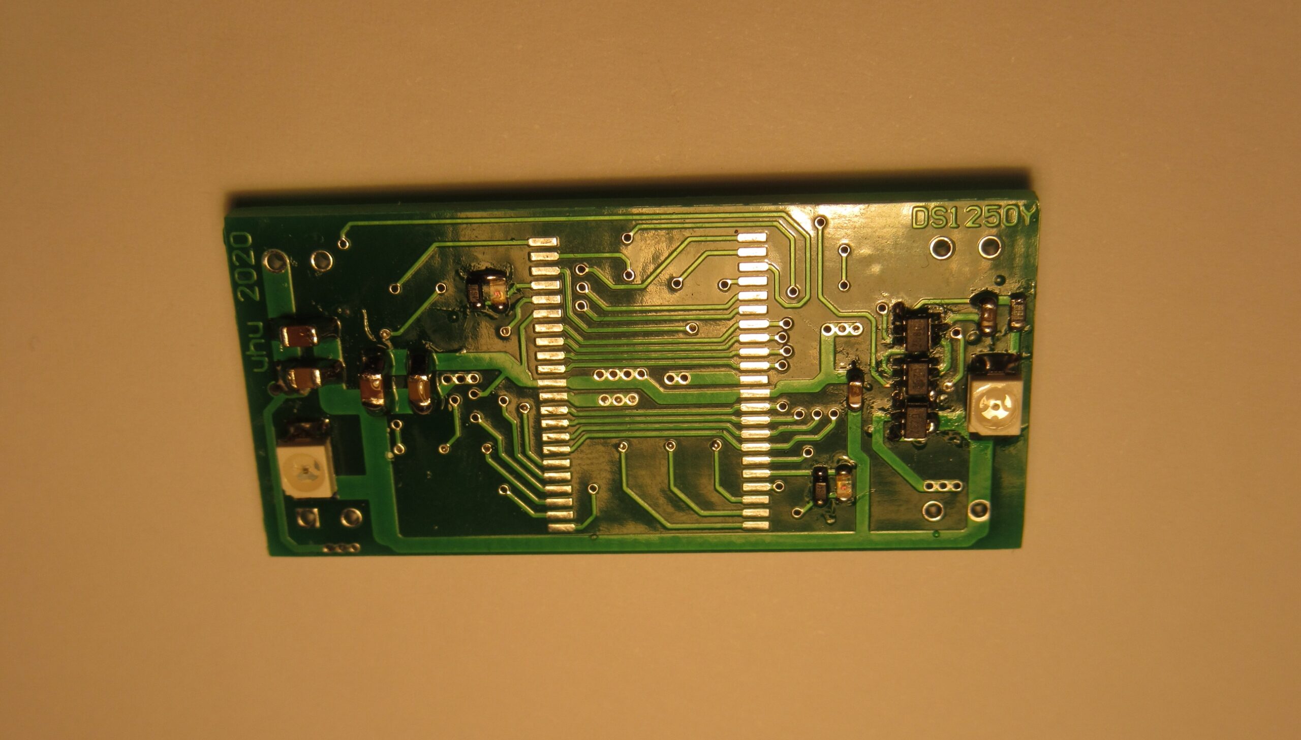
Finished boards are there and are assembledComponents manually assembled and solderedBottom viewBottom view, afterwards added pull ups connected with wire, modification added to published designBottom view, pin header fiddly soldered from besideFirst prototype in the programmer
We have a receiver in our living room that is almost exactly 50 years old. The Sony STR-V5 has a lot of oomph, is wired with wire-wrap connections like earlier space technology and will certainly work for another 50 years. The only problem was that its cinch inputs are no longer compatible with current devices that transmit wirelessly. This gave rise to the idea of building a slightly better Bluetooth receiver for the Sony with a matching retro look. The end result can already be seen here.
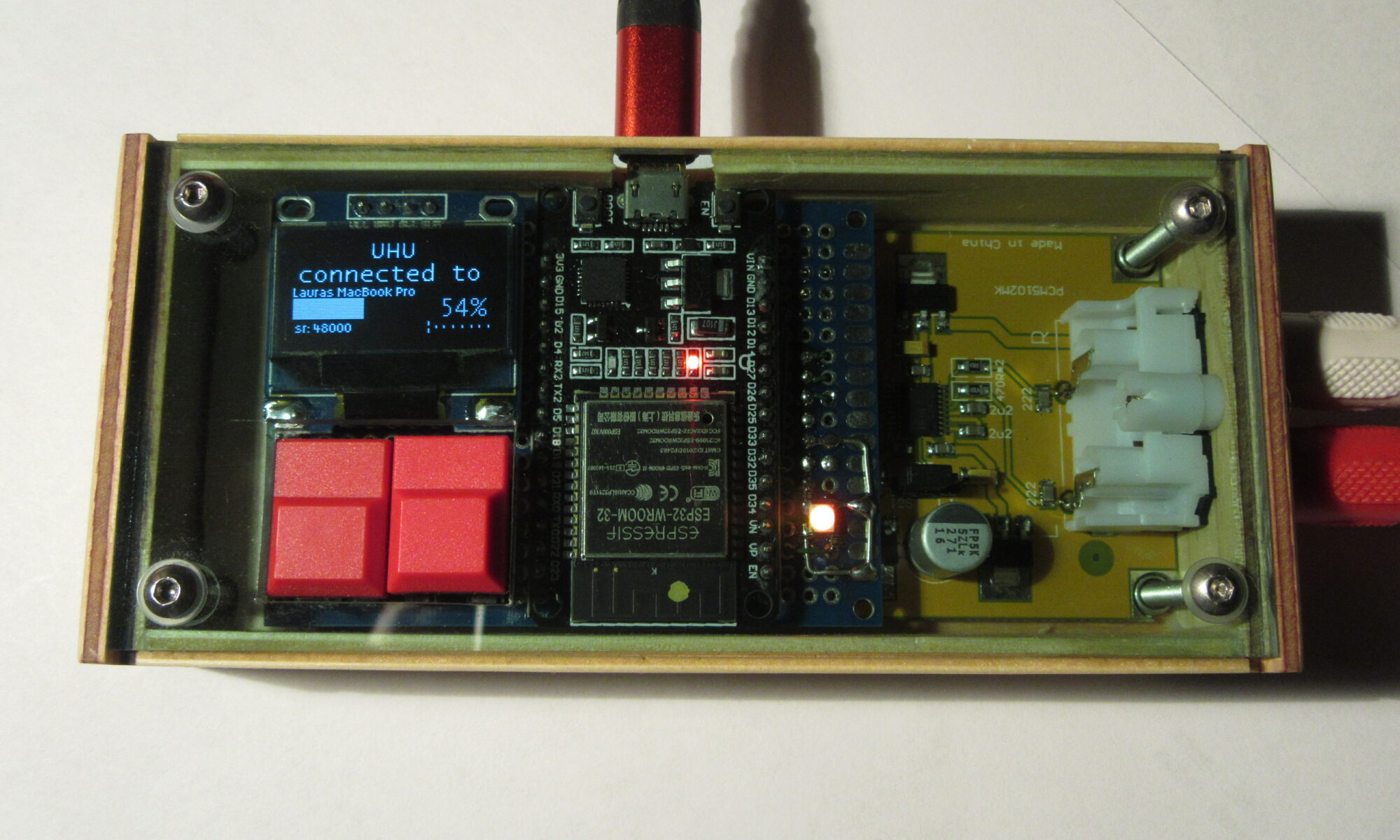
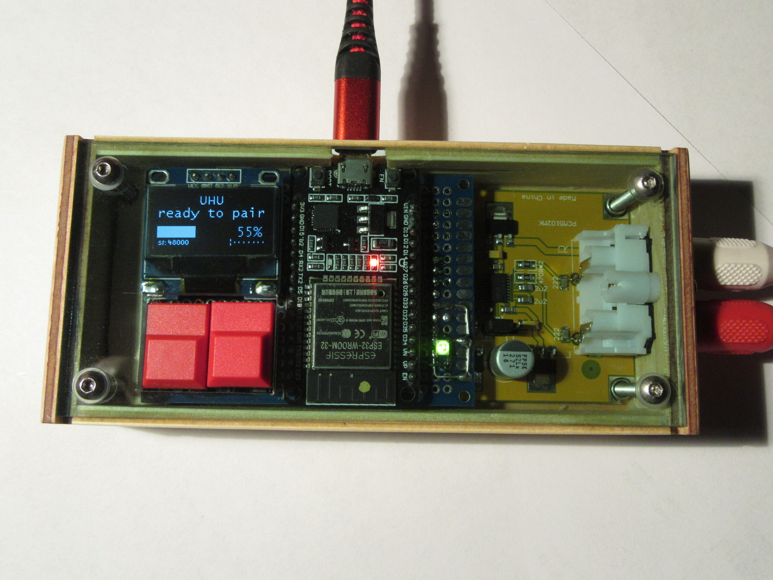
receiver ready
Bluetooth-Audio
Before this project, I had no idea about bluetooth. In my mind, it sounded pretty easy to transfer the audio and then play it back. Unfortunately, it’s not quite like that. Due to the limited data rate of a Bluetooth wireless connection, the data must be compressed. A “codec” does this. Of course, it has to be the same on the sending and receiving side. The oldest and currently the most widely used codecs are “AAC” and “SBC”. Audiophile users were not satisfied with the quality of this compression, so a number of new standards are trying to enter the market. In addition to “SBC” and “AAC”, “aptX”, “aptX HD” and “LDAC” are now also competing for the customer’s favor. Don’t forget: sender and receiver must support the same codec. For example, if you buy Bluetooth headphones with “aptX”, but the receiver speaks “LDAC”, only a connection with “SBC” is established, if it works at all.
Overall, the Bluetooth standard is quite complex and my interest in delving further into it is limited.The software uses “SBC”, which is supported by almost all devices.
Volume control
While programming, I noticed that the volume control with Bluetooth is the crux of the matter. The basic problem is that the audio samples are transmitted with 16 bits and usually 100% volume. In the receiver, the volume is now reduced to say 35%. That means we have to divide the audio samples roughly by 16. As a result, we have audio data with a resolution of only 12 bits. And that’s exactly how it sounds.
A simple solution to the problem is a 32 bit D/A converter. The received 16 bit samples are converted into 32 bit values by simply adding zeros. It doesn’t make a difference at first. In the second step, however, we can calculate the volume with the 32-bit value and then send it directly to the D/A converter. As a result, there is no loss of information at low volume, the 16-bit information is retained.
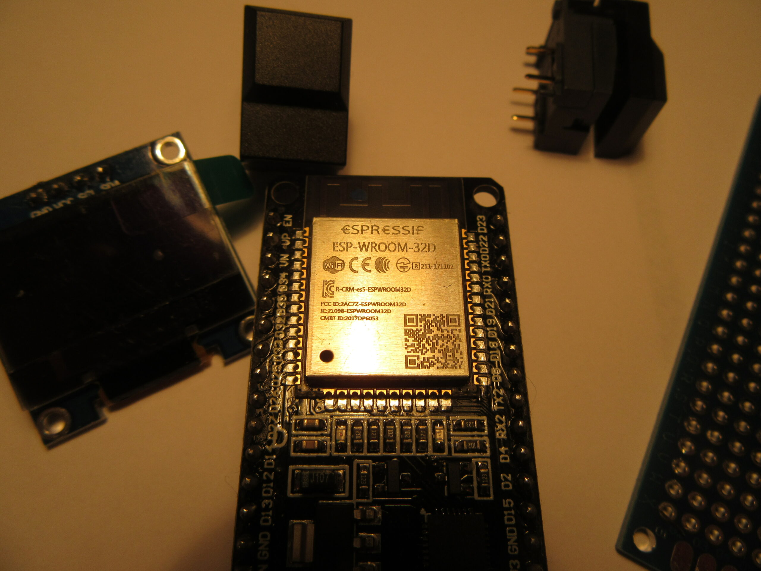
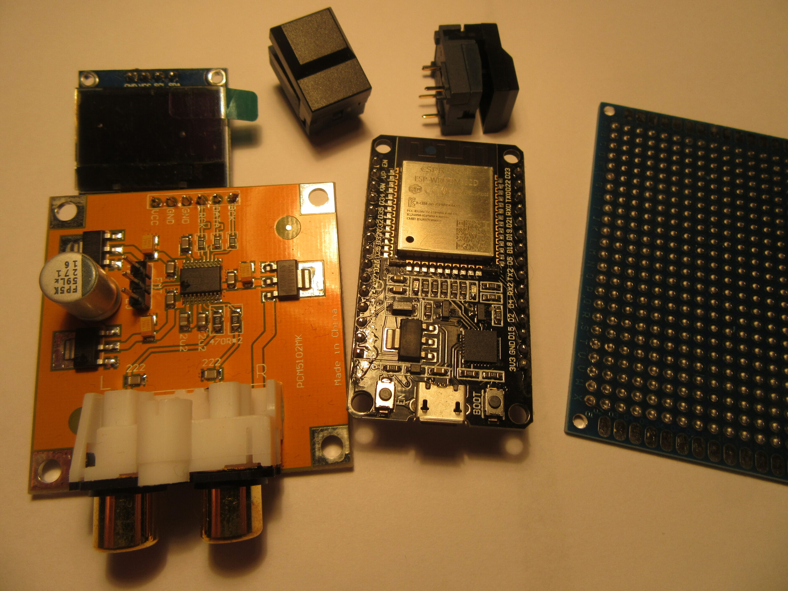
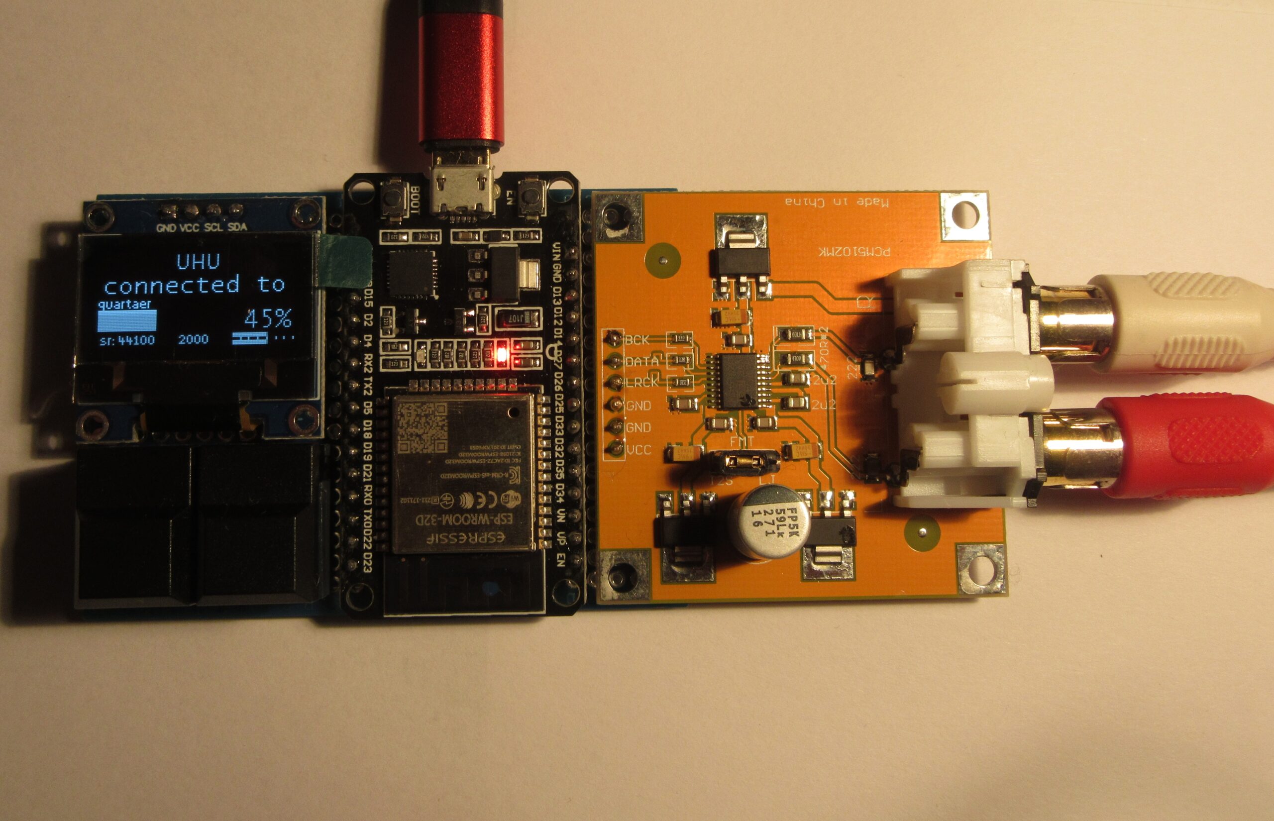
The heart of the circuit is an ESP32 microcontroller from Espressif. The system not only offers plenty of computing power for 3.50 euros, but is also energy-saving. There are a lot of code examples from the manufacturer and lively discussions in forums, which make application development and troubleshooting easier.
ESP-WROOM-32D module
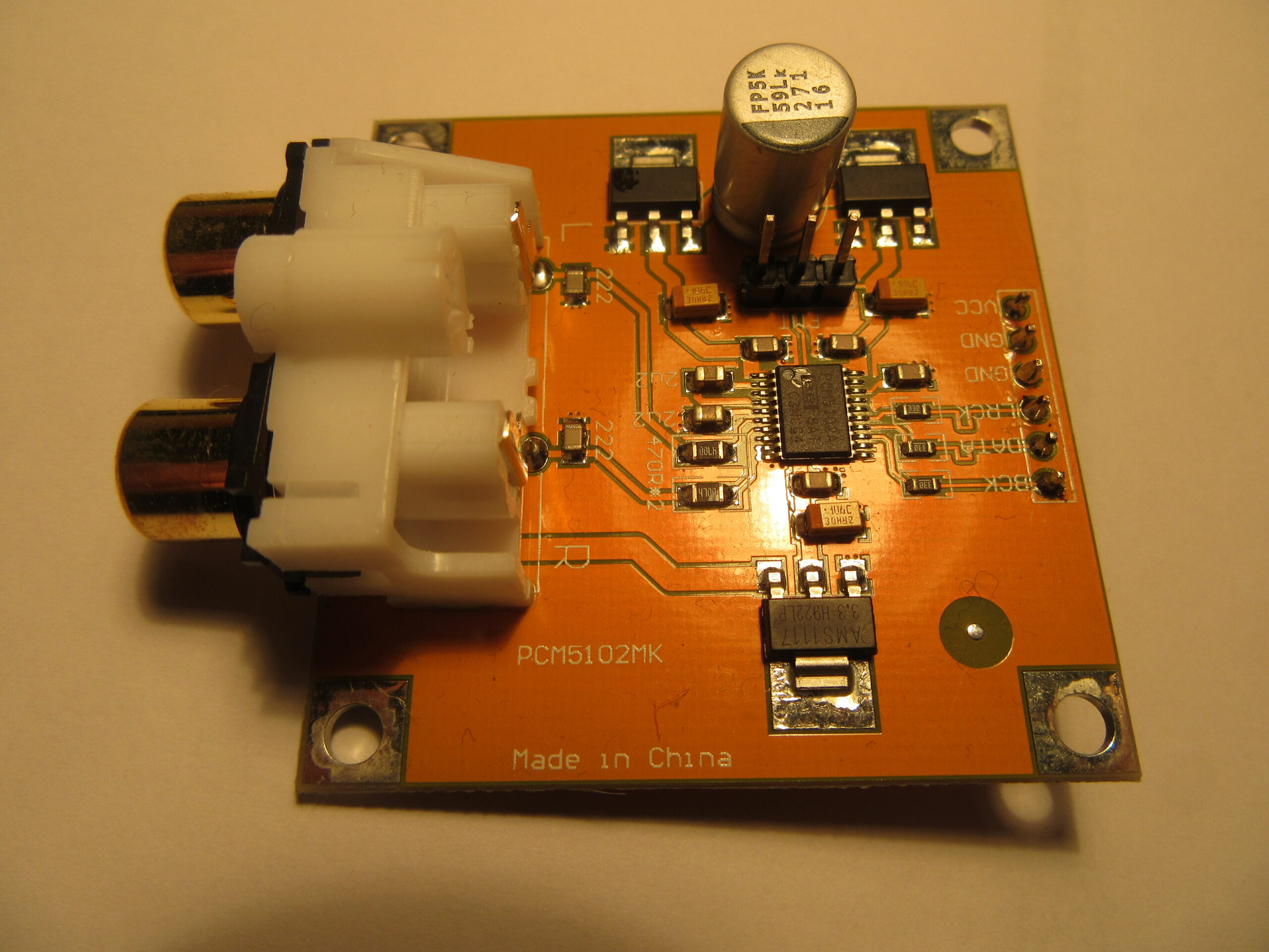
A PCM5102A from Texas Instruments with 32 bit and 112dB signal-to-noise ratio is used as a high-quality D/A converter. It’s actually way too good for Bluetooth audio, but the advantages of 32-bit pay off when it comes to volume control.
D/A converter board
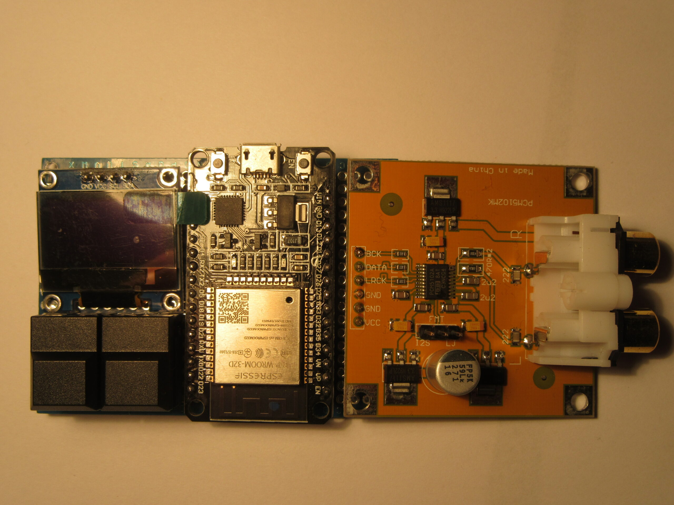
The whole is complemented by two buttons for volume and reset, a 128×64 pixel OLED display and a breadboard. For this project, I use ready-made modules that only need to be connected to each other. This is of course much faster than drafting your own circuit board.
components
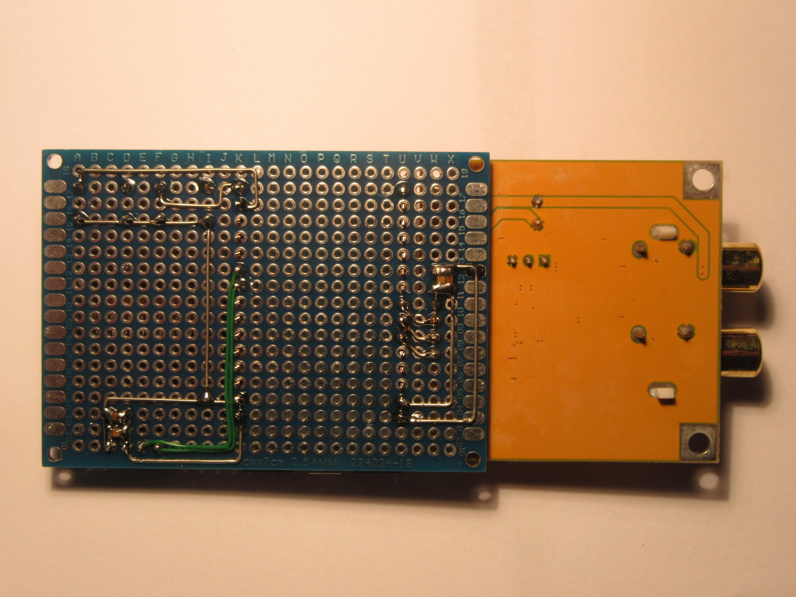
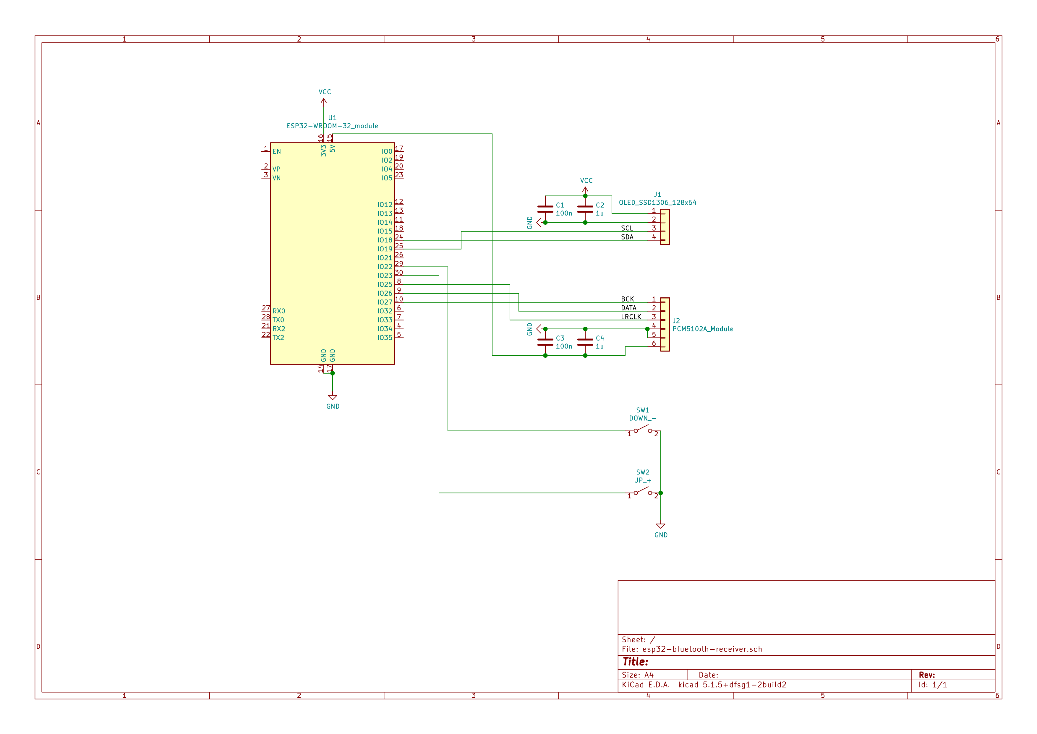
Circuit
Since I used finished modules for the project, the circuit is limited to a few connections between the central ESP32 module and the OLED display, the D/A converter and the two buttons. The whole thing is soldered together in an hour.
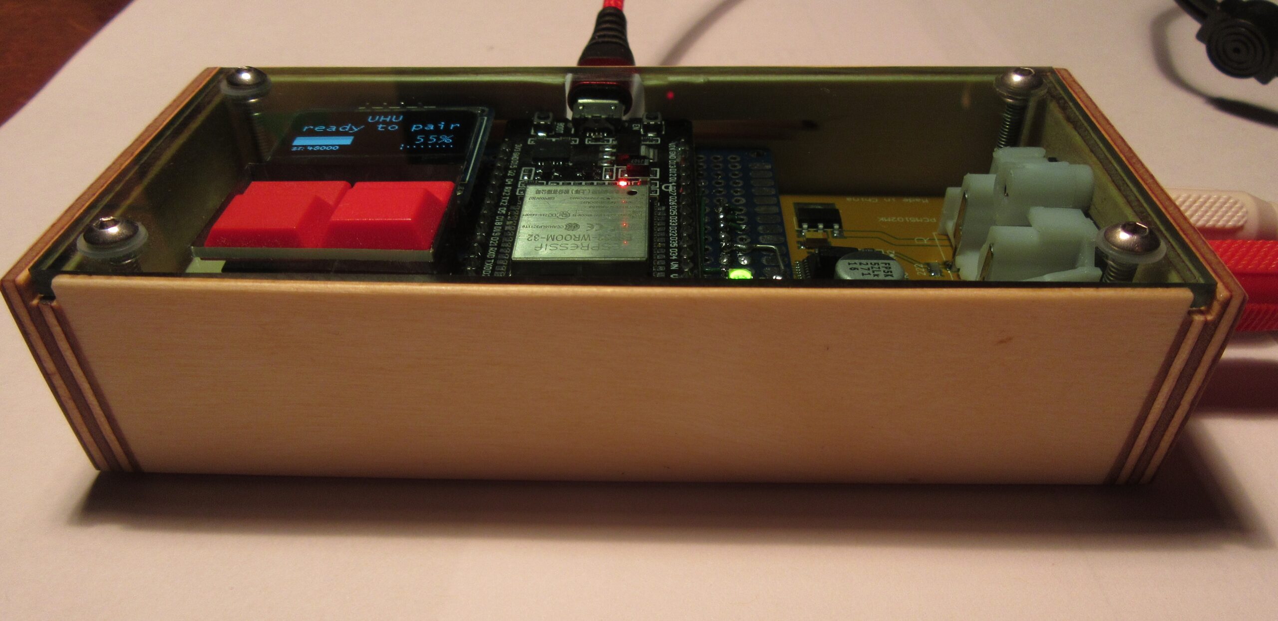
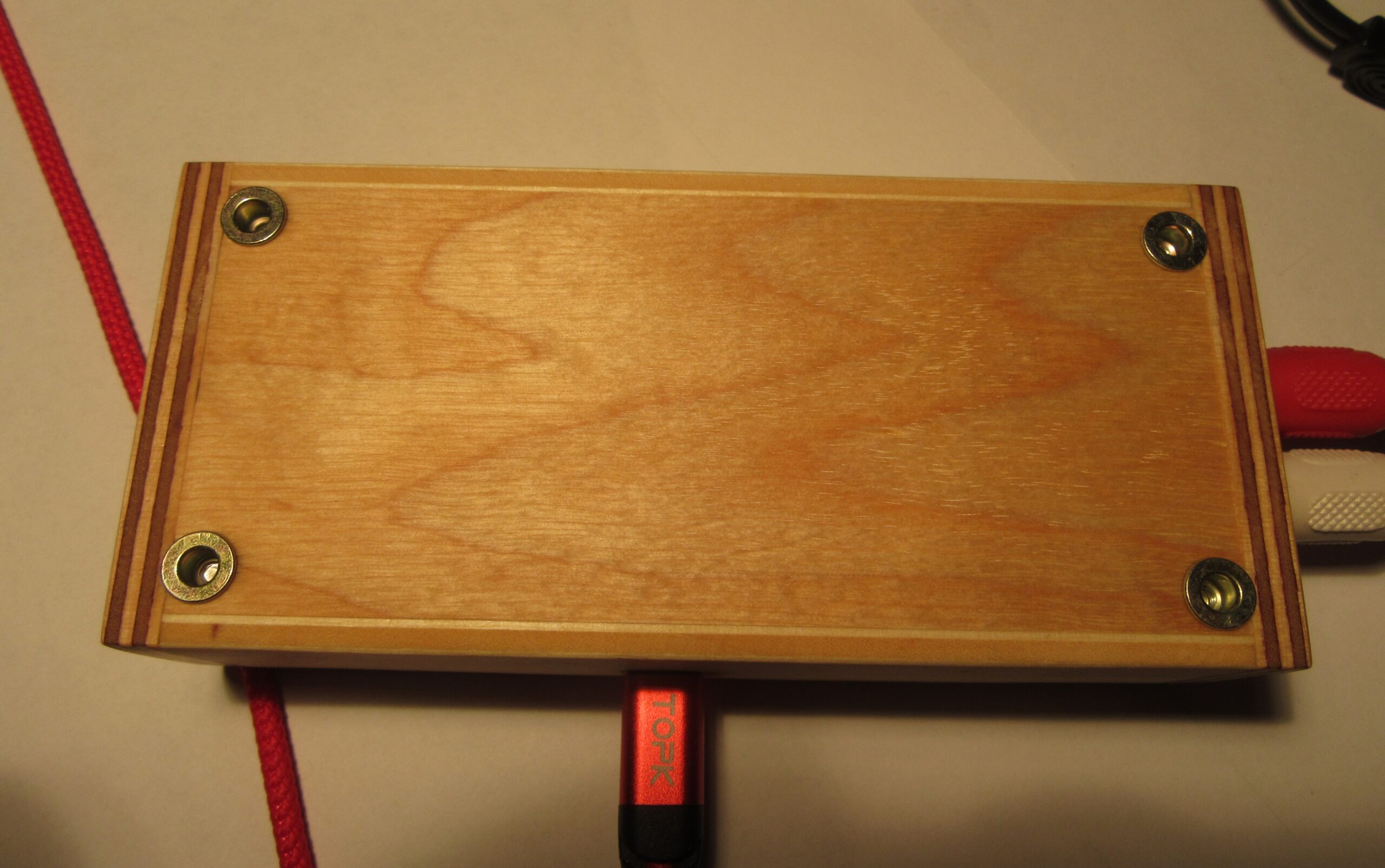
I built a small housing from glued plywood scraps, which has become very chic and goes well with the Sony receiver for my taste.
case made of plywood, front and bottom
Software
The software is derived from the example “A2DP-SINK” from the ESP32 manufacturer Espressif. That shortened the development time a lot for me, as the complete and rather complex Bluetooth communication is already implemented in the example. I added processing of the audio samples for volume control and the conversion from 16 to 32 bits as described above. I also added the routines for the OLED display. The operating status, the connected device and a logarithmic level display are shown on the display.
In the end, the programming and troubleshooting took a lot longer than a weekend, as a lot of bugs had to be found and fixed.
I have published the full source code, the instruction manual and guidance for compiling the project on Github.
I recently put together a Bluetooth audio receiver as a weekend project.At some point I got to the point of regulating the volume and had to realize that it is not that easy to do it well.As always, I researched the Internet for a while, in the end I had to experiment myself, true to the motto that you can’t program anything sensible that you don’t understand.
Volume and hearing
Our ear is an impressive organ. The audible range from the softest sound to the greatest noise spans about 6 decades. This means that the slightest sound is a million times quieter than the loudest we can hear. Since there is no physical upper limit for noise, the volume of hearing is set as the maximum, which we can hear for a short time without permanent damage.
Another important fact is that we can differentiate quieter sounds much better in terms of volume. This is noticeable in the fact that we can hear differences in volume very well with soft tones. The louder it gets, the less we notice a change.
This results in the following requirements for a good volume control: In the quiet area you have to be able to set very precisely in very small steps. The louder it gets, the bigger the steps and the change.
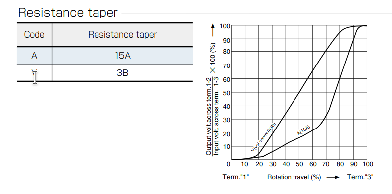
Of course, this was already known almost 100 years ago, and volume controls or potentiometers with a so-called logarithmic curve are built into even ancient analog electronics. On old potentiometers, for example, there is still “100kΩ log” for 100 kiloohms with a logarithmic course or e.g. “1M lin” for 1 megaohm and a linear course. On current models, the gradient is usually identified with the first letter:
“A20k” corresponds logarithmically, 20kΩ
“B2k” means linear 2kΩ
“C50k” means anti-logarithmic 50kΩ
With the advent of digital technology, however, some engineers did not do their homework and there are many (digital) devices in which the volume control does not work properly.Often the gradation in the lower range is too coarse, sometimes there are too few levels with 32 or even fewer setting levels.
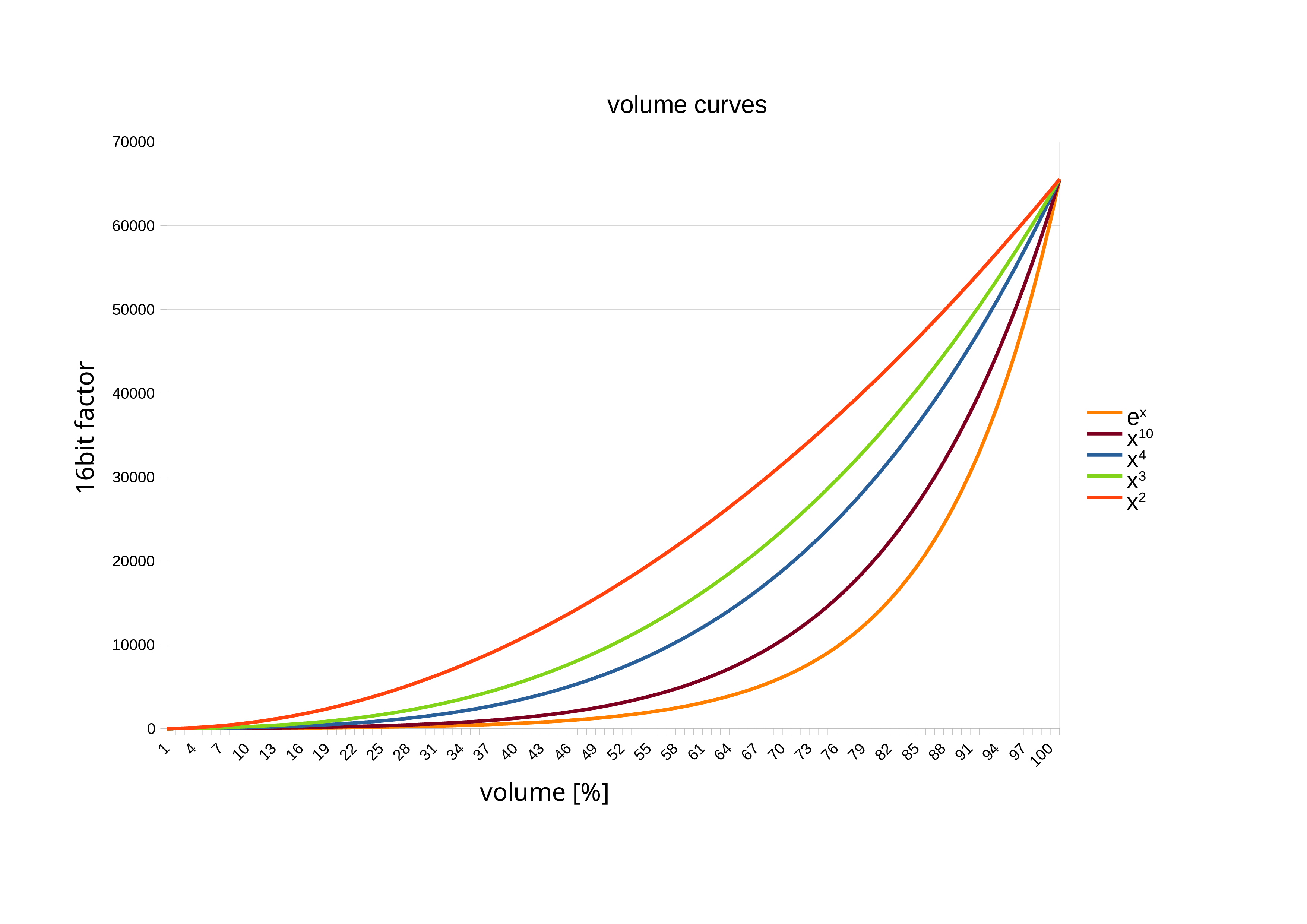
Comparison of different functions
As far as I know, a logarithmic curve for a volume control or a potentiometer is not exactly mathematically defined. According to the data sheets of some manufacturers, the resistance curves are partly linear with smooth transitions. For example, a manufacturer of high-quality audio potentiometers (Alps Alpine) has a curve with three linear ranges; flat up to almost 25%, a little steeper up to 65% and very steep at more than 65% angle of rotation.
One could of course relate to this digitally, but that would be relatively time-consuming. A math function is of course much easier to program.
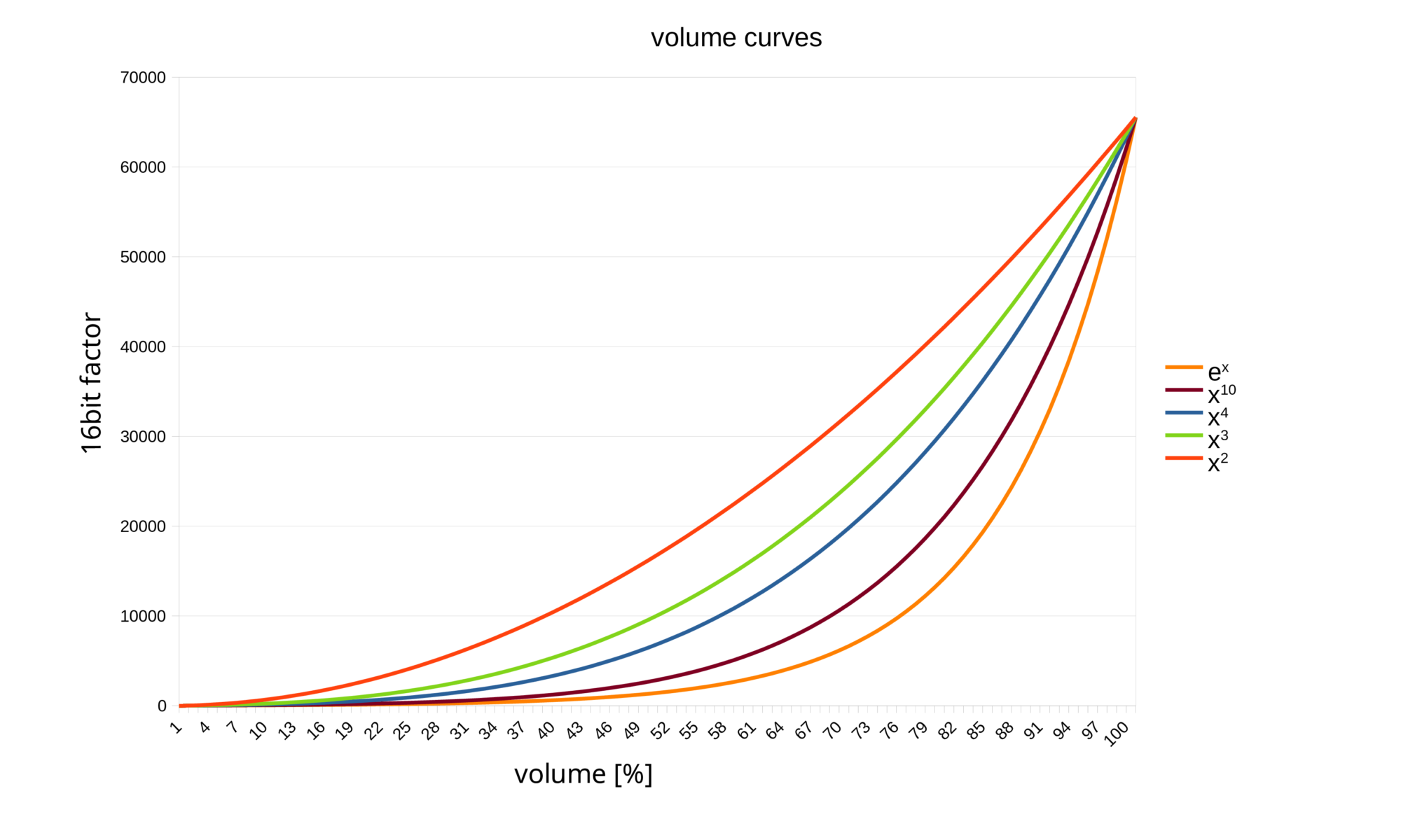
The desired curve shape, i.e. flat at the beginning, steep at the end, follows more of an exponential function or power functions. The higher the potency, the flatter the rise in the lower area and the steeper at the end. I tried different functions, first displayed the curves, then tested them by ear.
Curves of suitable volume functions
Optimal function
Judging by my ear, the function y = x³ has proven to be optimal. I also add a small offset so that the regulation begins in the lower range around the hearing threshold.
Calculation of the volume
To regulate the volume of digital audio data, a factor is normally used by which each audio sample is multiplied. If you work with floating point numbers, the factor is usually between 0 and 1. With fixed point arithmetic, the factor can be completely different. In the following an example as a C code, where the volume factor is a 16 bit value between 0 and 65536 and is calculated with the function y = x³.
If you multiply this value by 16-bit audio samples, you get 32-bit values as the result. I use this in a Bluetooth receiver, where 16-bit audio is received via Bluetooth and, after volume calculation, is output to a 32-bit PCM5102A D / A converter without loss of quality.
#include <stdint.h>
#include <stdlib.h>
#include <math.h>

//use x^3 function
#define VOL_POWER 3.0
//upper/lower limit of factor to multiply with samples
#define VOL_MIN 30.0
#define VOL_MAX 65536.0

//precalculate constants once
static const float vol_pow_min = pow(VOL_MIN, (1.0 / VOL_POWER));
static const float vol_pow_diff = pow(VOL_MAX, (1.0 / VOL_POWER)) - pow(VOL_MIN, (1.0 / VOL_POWER));

//calculate volume factor with power function
//argument vol: 0..100%
static uint32_t vol_calc(uint8_t vol) {
    if (vol == 0) return 0;
    if (vol >= 100) return VOL_MAX;

    return floor(pow((vol_pow_min + vol_pow_diff / 100 * vol), VOL_POWER));
}
As a little calculation aid and for your own experiments, my table with the series of numbers and experiments can be downloaded here: volume_calc.ods